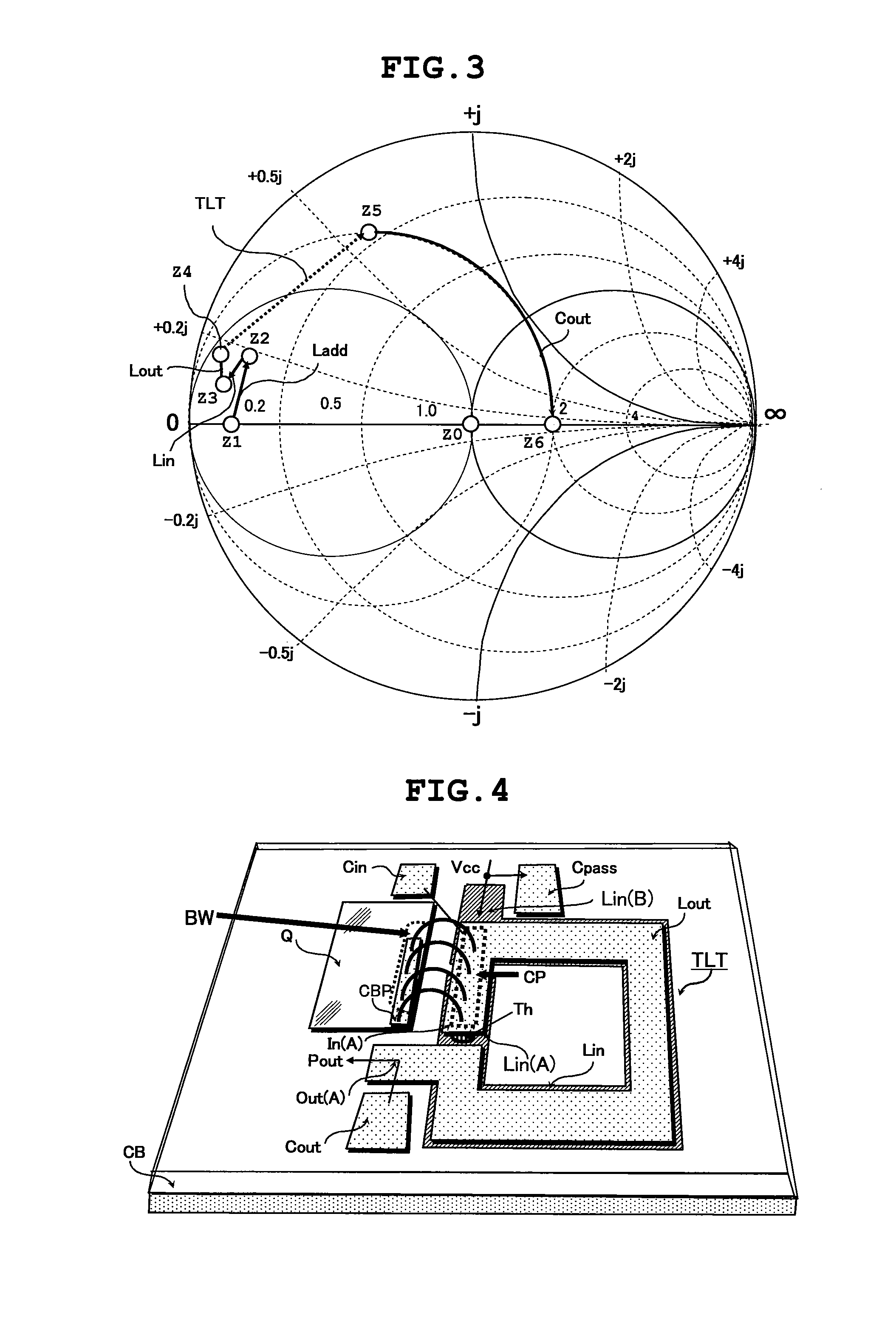
[0015]Further, as is well known, for supplying transmission power at a low
power supply voltage to a 50-Ω antenna of mobile communications equipment such as a
cellular telephone, and so forth, an impedance matching circuit is coupled between an output of the
RF power amplifier, and the antenna as the load thereof. By use of, for example, a lossless transformer having a
transformation ratio of 1:4 as the impedance matching circuit, a peak-to-peak amplitude at 5 V of the
RF power amplifier will be turned to a peak-to-peak amplitude at 20 V. In other words, with the use of the transformer as the impedance matching circuit, load impedance can be effectively converted lower in value, so that it is possible to output a target transmission power even at a limited amplitude outputted by the
RF power amplifier.
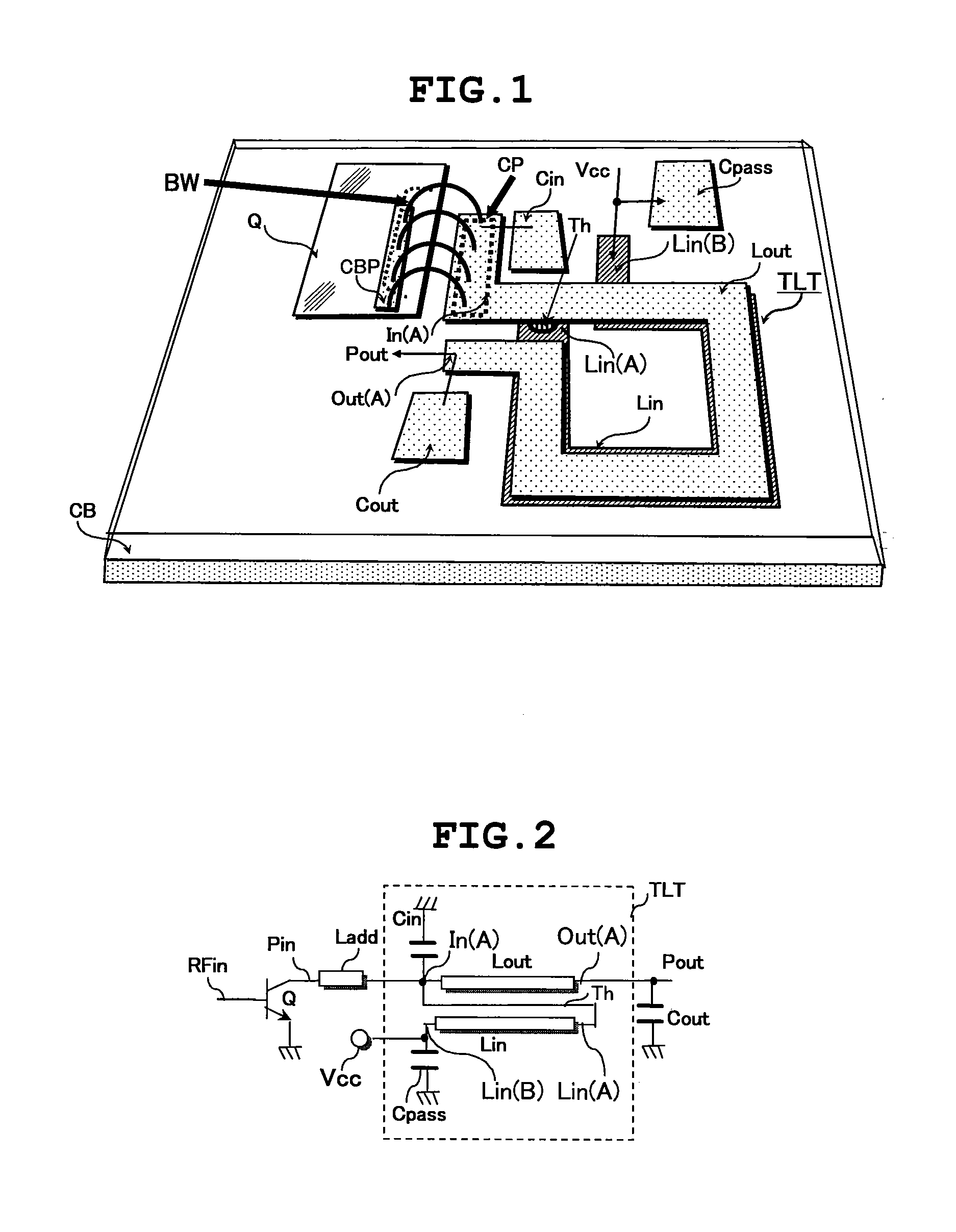
[0020]Accordingly, due to impedance conversion from the secondary line Lin of the transmission line transformer TLT to the main line Lout, conversion output power of the power hetrojunction bipolar transistor (HBT) Q can be generated from the other end Out (A) of the main line Lout of the transmission line transformer TLT. That is, a
characteristic impedance is developed by the agency of the interlayer
dielectric disposed between the secondary line Lin of the transmission line transformer TLT and the main line Lout. Accordingly, an inductive-
capacitive coupling energy is transmitted in a transmission line mode from the secondary line Lin of the transmission line transformer TLT to the main line Lout. Therefore, it becomes possible to take out an RF amplified
voltage signal from an output electrode of an
amplifier element without the use of an air-core coil as a
load circuit, and without the use of a
spiral coil, or
choke inductance, having a large current-
carrying capacity and a high
Q factor.
[0021]The power hetrojunction bipolar transistor (HBT) Q is formed over an III-V group
compound semiconductor chip, and for the power hetrojunction bipolar transistor (HBT) Q, use is made of a hetrojunction bipolar transistor of, for example, GaAs, and InP. Further, as another HBT, use can be made of an SiGe hetrojunction bipolar transistor formed over a
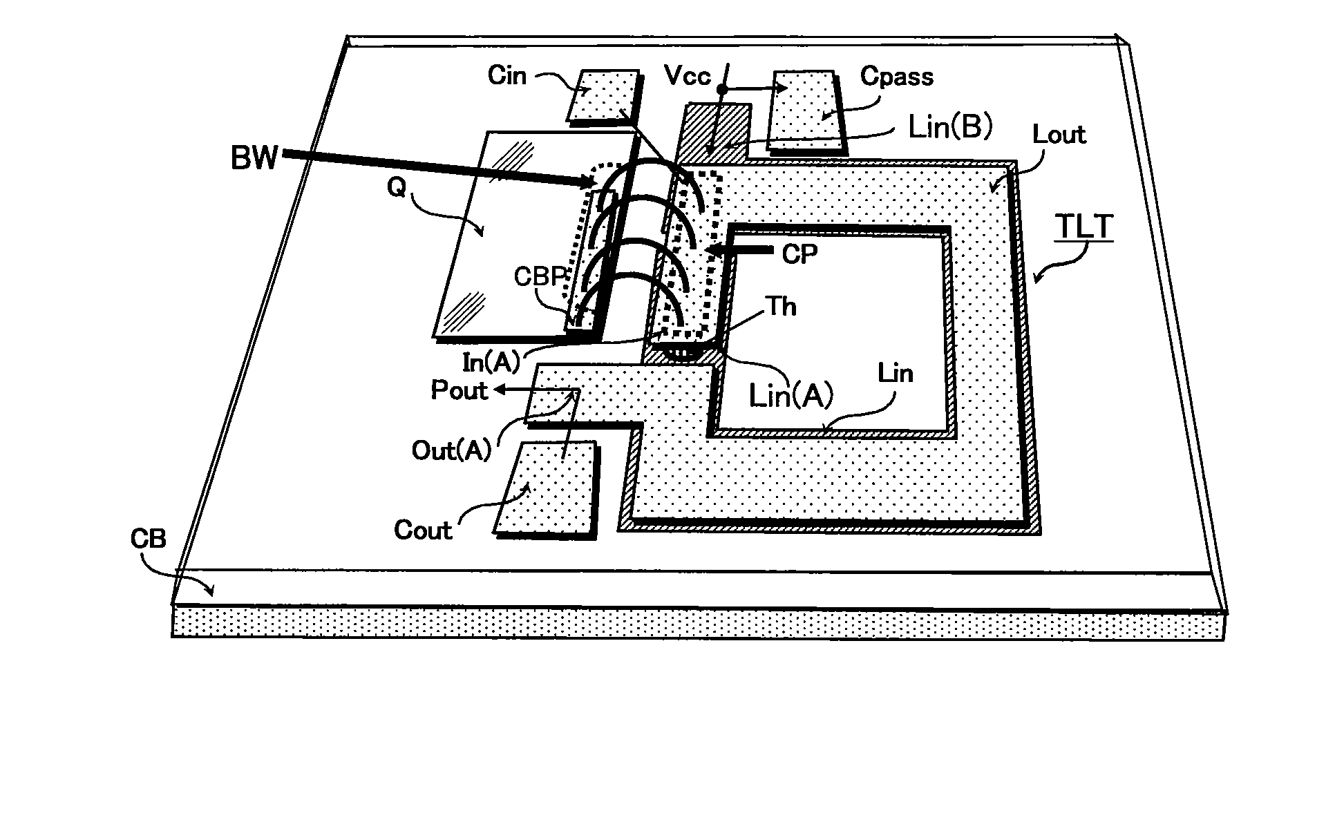
silicon substrate, as well. Accordingly, the collector output electrode of the power hetrojunction bipolar transistor (HBT) Q is formed of an
interconnection layer CBP fabricated on the surface of the III-V group
compound semiconductor chip, or on the surface of a
silicon semiconductor chip by a
semiconductor manufacturing process. The collector output electrode CBP of the power hetrojunction bipolar transistor (HBT) Q is coupled to a joint CP of the main line Lout as the upper-level
interconnection formed over the main surface of the circuit board CB of the RF
power module via four bonding wires BW coupled in parallel. Low parasitic resistance and low parasitic
inductance, caused by the four bonding wires BW coupled in parallel, will reduce a
voltage drop owing to a collector current of the power hetrojunction bipolar transistor (HBT) Q on the order of an
ampere. In this connection, the joint CP of the main line Lout as the upper-level interconnection is a bonding pad for the four bonding wires BW.
[0022]That is, the joint CP of the bonding pad is formed so as to be isolated from an energy transmission /
coupling part for inductive-
capacitive coupling, located between the transmission line of the main line Lout, and the transmission line of the secondary line Lin of the transmission line transformer TLT. A first reason as the main reason for isolation described as above is to lessen effects of magnetic fluxes of an RF frequency generated from the four bonding wires BW coupled to the joint CP of the bonding pad on the energy transmission coupling part between the transmission line of the main line Lout, and the transmission line of the secondary line Lin, of the transmission line transformer TLT. A second reason for the isolation is to lesson effects of
mechanical pressure exerted by a wire bonder in the step of
wire bonding with the bonding wires BW at the time of manufacturing the RF
power module on the interlayer
dielectric disposed between the secondary line Lin, and the main line Lout, of the transmission line transformer TLT. That is, taking into consideration a possibility of a crack occurring to the interlayer
dielectric due to the pressure exerted by the wire bonder, or electrical insulation properties of the interlayer dielectric undergoing deterioration due to occurrence of a crack, the joint CP of the bonding pad is formed so as to be isolated from the energy transmission coupling part.
[0040]That is, a condition for impedance matching of the transmission line transformer can be maintained when the output electrode of the power transistor in the final amplifying stage is joined with the transmission line transformer serving as the impedance matching circuit.
