Evaporation Donor Substrate and Method for Manufacturing Light-Emitting Device

a donor substrate and light-emitting technology, applied in applications, transportation and packaging, other domestic articles, etc., can solve the problems of increasing the number of pixels, achieve the effect of improving productivity, facilitating and accurately deposited, and fully automating the deposition process

Inactive Publication Date: 2009-04-23
SEMICON ENERGY LAB CO LTD
View PDF23 Cites 46 Cited by
  • Summary
  • Abstract
  • Description
  • Claims
  • Application Information

AI Technical Summary

Benefits of technology

[0015]The present invention provides an evaporation donor substrate which is used for deposition by an evaporation method and which allows only a desired portion of an evaporation material to be evaporated so that use efficiency of the evaporation material is increased to reduce manufacturing cost, and so that a film with high uniformity to be deposited.
[0016]In addition, the present invention provides, by using such an evaporation donor substrate, a method for manufacturing a light-emitting device by which higher definition (an increase in the number of pixels) and miniaturization of pixel pitches along with downsize of the light-emitting device can be advanced.
[0026]By using an evaporation donor substrate according to the present invention, the thickness of the film formed onto a deposition target substrate during the deposition can be controlled by controlling the thickness of a material layer which is formed over the evaporation donor substrate. Therefore, a user does not have to adjust an evaporation speed with a thickness monitor, and the deposition process can be fully automated. Accordingly, productivity can be improved.
[0027]In addition, by using an evaporation donor substrate according to the present invention, an evaporation material contained in the material layer which is formed over the evaporation donor substrate for deposition can be uniformly sublimed. In the case where the material layer contains plural kinds of evaporation materials, a film containing the same evaporation materials at roughly the same weight ratio as the material layer can be deposited onto the deposition target substrate. Therefore, in deposition using an evaporation donor substrate according to the present invention, when deposition is performed using plural kinds of evaporation materials having different evaporation temperatures, unlike co-evaporation, the evaporation rate of each evaporation material does not have to be controlled. Thus, without complicated control of the evaporation rate or the like, a desired layer containing different kinds of evaporation materials can be deposited easily and accurately.
[0028]In addition, by a deposition method using an evaporation donor substrate of the present invention, a flat and even film can be deposited, and a minute pattern can be formed; thus, a high-definition light-emitting device can be obtained. Further, in the present invention, a lamp heater or the like with large energy power can be used as a light source. By use of a lamp heater or the like as a light source, deposition can be performed over a large area at a time; thus, a cycle time can be shortened compared with the case of, for example, using a laser device as a light source. Accordingly, manufacturing cost of a light-emitting device which is manufactured employing a deposition method using an evaporation donor substrate according to the present invention can be reduced.
[0029]By manufacturing a light-emitting device including a light-emitting element using an evaporation donor substrate according to the present invention, use efficiency of an EL material is improved, whereby manufacturing cost can be reduced. In addition, formation of an EL layer of a light-emitting element into a desired shape with high accuracy can be facilitated; accordingly, characteristics of the light-emitting device can be improved.

Problems solved by technology

Such needs are major problems in advancing high definition (increasing the number of pixels) and miniaturization of pixel pitches along with downsize of a light-emitting device including a light-emitting element.

Method used


Image

  • Evaporation Donor Substrate and Method for Manufacturing Light-Emitting Device
  • Evaporation Donor Substrate and Method for Manufacturing Light-Emitting Device
  • Evaporation Donor Substrate and Method for Manufacturing Light-Emitting Device

Examples


embodiment mode 1

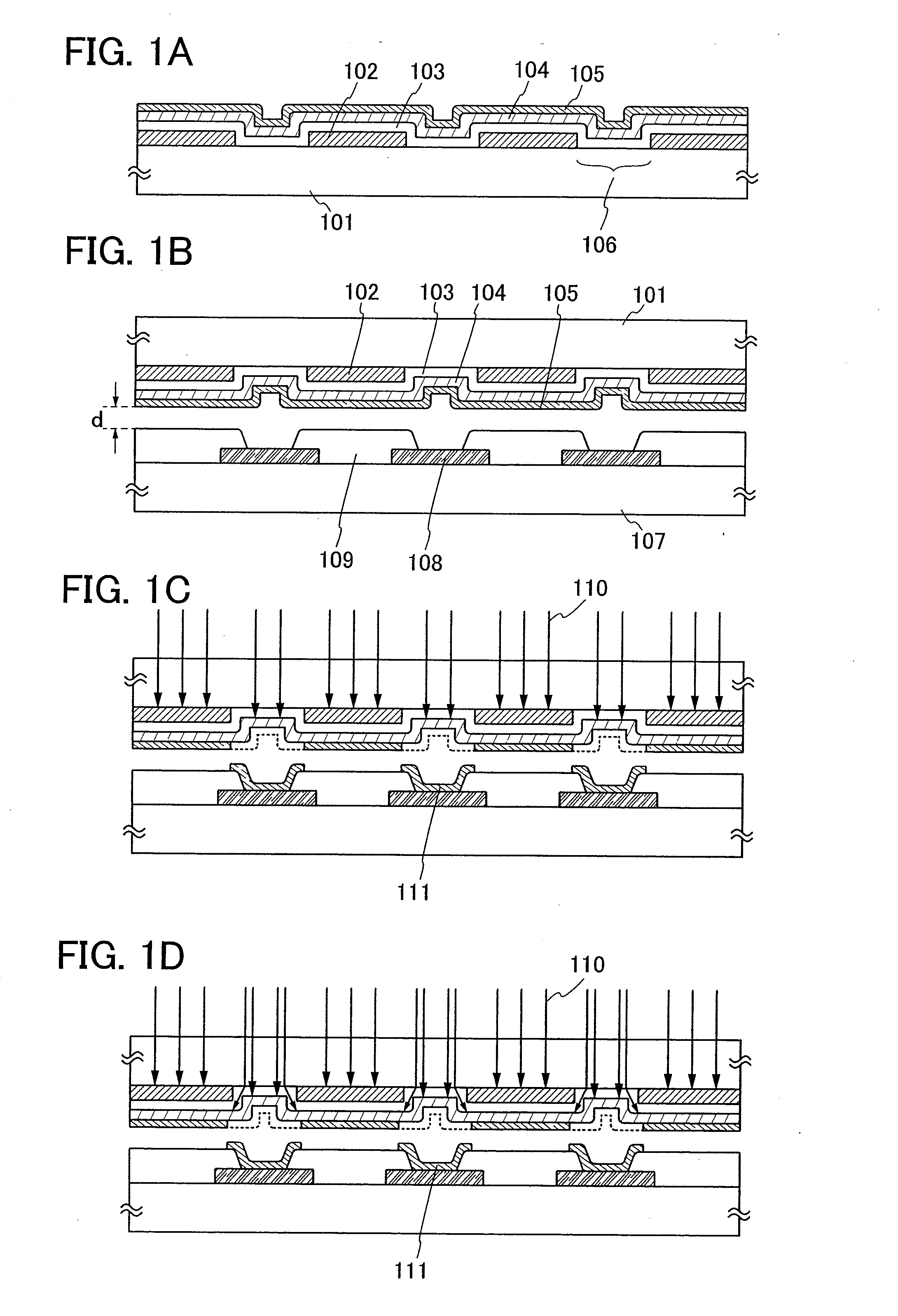
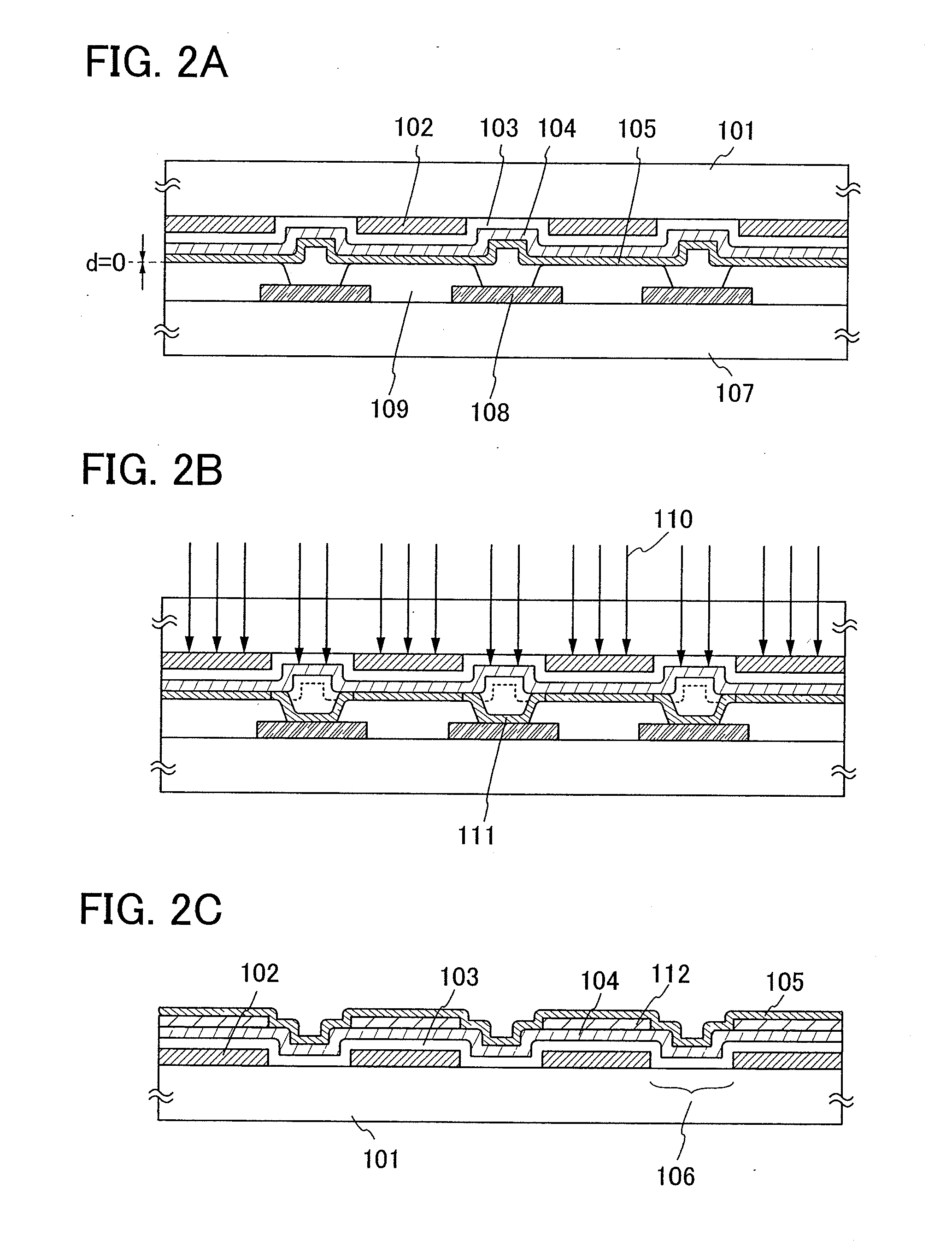
[0046]Embodiment Mode 1 describes an evaporation donor substrate according to the present invention and a deposition method using the evaporation donor substrate. Note that Embodiment Mode 1 describes a case where an EL layer of a light-emitting element is formed using an evaporation donor substrate.

[0047]As shown in FIG. 1A, a reflective layer 102 is formed over a first substrate 101 which is a supporting substrate. Note that the reflective layer 102 has an opening 106. A heat insulating layer 103 is formed over the reflective layer 102. Note that the heat insulating layer 103 is formed so that a part thereof fills the opening 106 of the reflective layer 102. A light absorption layer 104 is formed over the heat insulating layer 103.

[0048]Further, a material layer 105 which is formed of an evaporation material is formed over the light absorption layer 104. In FIG. 1A, the heat insulating layer 103, the light absorption layer 104, and the material layer 105 are formed over the entire...

embodiment mode 2

[0091]Embodiment Mode 2 describes a method for manufacturing a light-emitting device which is capable of full-color display by forming an EL layer of a light-emitting element with a plurality of evaporation donor substrates which are described in Embodiment Mode 1.

[0092]While Embodiment Mode 1 describes the case in which an EL layer of the same kind of material is formed onto all of the plurality of electrodes over a second substrate, which is a deposition target substrate, through one deposition process, Embodiment Mode 2 describes the case in which EL layers of three different color emission are formed onto the plurality of electrodes over the second substrate.

[0093]First, three evaporation donor substrates each of which is the evaporation donor substrate in FIG. 1A in Embodiment Mode 1 are prepared. Note that a material layer containing an evaporation material for forming EL layers of a different emission color is formed in each evaporation donor substrate. Specifically, a first ...

embodiment mode 3

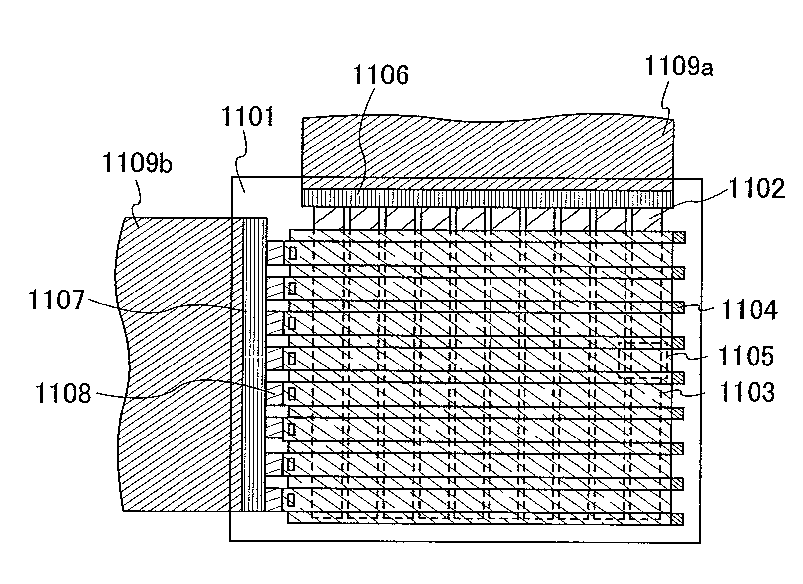
[0111]This embodiment mode describes examples of deposition apparatuses with which the light-emitting device according to the present invention can be manufactured. FIGS. 6A and 6B and FIGS. 7A and 7B show schematic cross-sectional views of deposition apparatuses of this embodiment mode.

[0112]In FIG. 6A, a deposition chamber 601 is a vacuum chamber and is connected to other treatment chambers via a first gate valve 602 and a second gate valve 603. The deposition chamber 601 at least includes an evaporation donor substrate supporting mechanism 604, a deposition target substrate supporting mechanism 605, and a light source 610.

[0113]First, in another deposition chamber, a material layer 608 is formed over an evaporation donor substrate 607. Here, as a supporting substrate which forms the evaporation donor substrate 607, a square plate substrate which includes copper as its main material is used. For the material layer 608, a material which can be evaporated is used. Note that there is...


PUM

PropertyMeasurementUnit
reflectanceaaaaaaaaaa
transmittanceaaaaaaaaaa
thicknessaaaaaaaaaa

Abstract

To provide an evaporation donor substrate which is used for deposition by an evaporation method and which allows reduction in manufacturing cost and high uniformity of a film which is deposited. In addition, to provide a method for manufacturing a light-emitting device using the evaporation donor substrate. The evaporation donor substrate includes a reflective layer having an opening which is formed over a substrate, a heat insulating layer having a light-transmitting property which is formed over the substrate and the reflective layer, a light absorption layer which is formed over the heat insulating layer; and a material layer which is formed over the light absorption layer.

Description

BACKGROUND OF THE INVENTION[0001]1. Field of the Invention[0002]The present invention relates to evaporation donor substrates used for deposition of materials which can be deposited by an evaporation method. In addition, the present invention relates to a method for manufacturing light-emitting devices which employs the evaporation donor substrate.[0003]2. Description of the Related Art[0004]Light-emitting elements which use organic compounds and are characterized by thinness, lightweight, fast response, and direct current low voltage driving, are expected to be applied as a light-emitter to next-generation flat panel displays. In particular, a display device in which light-emitting elements are arranged in matrix has an advantage in a wide viewing angle and excellent visibility over a conventional liquid crystal display device.[0005]A light emission mechanism of a light emitting element is described below: when voltage is applied between a pair of electrodes with an EL layer interp...

Claims


Application Information

Patent Timeline
Patent Type & Authority Applications(United States)
IPC IPC(8): B32B3/24B05D5/06C23C16/48
CPCB32B7/02Y10T428/24331C23C14/24C23C14/28C23C14/568H01L27/3211H01L51/0013H01L51/56H05B33/10B32B2255/00B32B2307/302B32B2307/40B32B2307/416B32B2457/206Y10T428/24314Y10T428/24298C23C14/12C23C14/048H10K59/35H10K71/18H10K71/00
Inventor AOYAMA, TOMOYASATO, YOSUKEYOKOYAMA, KOHEITAKAHASHI, RENA
Owner SEMICON ENERGY LAB CO LTD
Why Eureka
Try Eureka