Semiconductor thin film and process for producing the same

a technology of semiconductors and thin films, applied in the direction of crystal growth process, inorganic chemistry, natural mineral layered products, etc., can solve the problems of large energy and a large number of steps, large switching speed, and large switching speed, and achieve excellent thermal stability, high transparency, and specific resistance

Inactive Publication Date: 2009-05-21
IDEMITSU KOSAN CO LTD
View PDF10 Cites 5 Cited by
  • Summary
  • Abstract
  • Description
  • Claims
  • Application Information

AI Technical Summary

Benefits of technology

[0046]As described above, the transparent oxide semiconductor obtained by the invention is excellent in thermal stability, maintains a specific resistance in the semiconductor region, and has a high transparency and a high mobility.
[0047]Also, according to the invention, the above-mentioned transparent oxide semiconductor can easily be obtained by controlling the concentration of oxygen when a film thereof is produced.

Problems solved by technology

However, when the silicon based thin film is amorphous, the film has drawbacks that the switching speed is relatively small and thus when high-speed moving images or the like are displayed, the switching element may not follow the movement thereof.
In the meantime, in the case of crystalline silicon based thin films, the switching speed is relatively large.
Thus, there remains a problem that a great deal of energy and a large number of steps are required.
However, it is known that when an electric current is caused to flow thereto, a change in characteristics thereof by the passage of time may become a problem.

Method used


Image

  • Semiconductor thin film and process for producing the same
  • Semiconductor thin film and process for producing the same

Examples


Embodiment Construction

[0050]Hereinafter, a preferred embodiment of the invention will be described on the basis of the drawings.

[0051](1) Preparation of the Production of Transparent Oxide Semiconductors

(Formation of Targets)

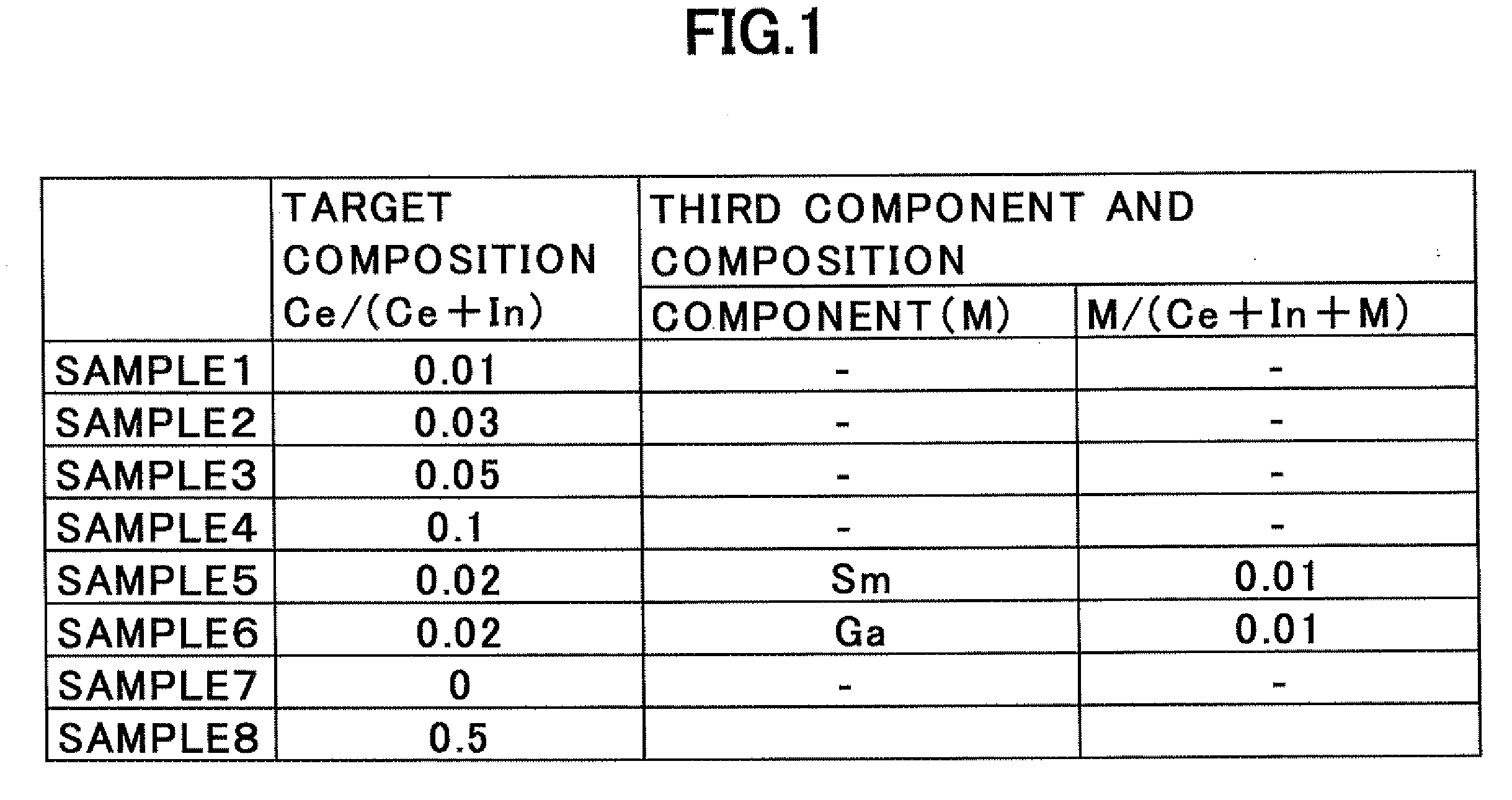
[0052]First, a target sample 1 was formed.

[0053]Powders (average particle diameter: 1 μm or less) of indium oxide and cerium oxide were charged into a wet ball mill vessel to set a mole ratio of Ce / (In+Ce) to 0.01, and then the powders were mixed and pulverized over 72 hours.

[0054]Next, the thus-obtained pulverized product was granulated, and then the resultant was press-molded into a size 4 inches in diameter and 5 mm in thickness. This was put into a firing furnace, and then heated at a temperature of 1400° C. for 36 hours to form a target.

[0055]Ce / (In+Ce) is an atomic number ratio, and this value is equal to the above-mentioned mole ratio in the present embodiment.

[0056]In the same manner, the composition of indium oxide and cerium oxide was changed to form target samples 2 to 8.

[...


PUM

PropertyMeasurementUnit
temperatureaaaaaaaaaa
particle diameteraaaaaaaaaa

Abstract

This invention provides a transparent oxide semiconductor, which comprises an oxide comprising indium oxide as a main component and cerium oxide as an additive and has such properties that light-derived malfunction does not occur, there is no variation in specific resistance of a thin film caused by heating and the like, and the mobility is high, and a process for producing the same. A semiconductor thin film characterized by comprising indium oxide and cerium oxide and being crystalline and having a specific resistance of 10+1 to 10+8 Ωcm is used. This semiconductor thin film has no significant change in specific resistance and has high mobility. Accordingly, an element having improved switching properties can be provided by constructing a switching element using this semiconductor thin film.

Description

TECHNICAL FIELD[0001]The present invention relates to a semiconductor device, in particular, a semiconductor element made of a crystalline thin film, and an application of the semiconductor element to a display device or the like.BACKGROUND ART[0002]In recent years, display devices have been remarkably developed, and various display devices such as a liquid crystal display device or an EL display device have been actively introduced into OA instruments such as a computer, flat television sets, and others. These display devices each have, as a basic structure, a sandwich structure wherein a display element is sandwiched between transparent conductive films.[0003]As switching elements for driving these display devices, elements each using a thin film are widely used from the viewpoint of downsizing or others.[0004]Hitherto, the thin film has been technically investigated about the composition thereof, the production process thereof, and others since the film produces a large effect on...

Claims


Application Information

Patent Timeline
Patent Type & Authority Applications(United States)
IPC IPC(8): H01L29/66H01L21/34
CPCC01G15/00C04B2235/6567C01P2006/40C23C14/086C23C14/3414C30B29/06C30B29/16H01L21/02565H01L21/02631H01L21/02667C04B35/01C04B2235/3224C04B2235/3229C04B2235/3286C01G15/006C23C14/08C23C14/34H01L21/34
Inventor INOUE, KAZUYOSHIYANO, KOKITANAKA, NOBUOTANAKA, TOKIE
Owner IDEMITSU KOSAN CO LTD
Why Eureka
Try Eureka