[0017]In one embodiment, the integrated image data for regions of non-uniformity are compared to the integrated image data for other parts of the wafer to determine if the non-uniformity results in a positive or negative change in surface potential or
capacitance. If a non-uniformity represents a change in surface potential, then the direction (positive or negative) of the
signal indicates whether the surface potential is increasing or decreasing. If a non-uniformity represents a change in surface height, then the direction of the
signal indicates whether the wafer height is increasing or decreasing. This information is then used to classify non-uniformities based on the direction of surface potential or surface height change. For example, surface
contamination may result in an increase or decrease in wafer surface potential. Many, but not all, types of
metal contamination on
silicon surfaces result in an increase in surface potential, while many types of organic
contamination on
silicon surfaces results in a decrease in surface potential. In inspection applications where likely
metal contaminants increase surface potential and likely organic contaminants decrease surface potential, the direction of surface
potential change can be used to distinguish between metallic surface contamination and organic surface contamination.
Independent data can be used to assist in determining the likelihood of contaminants or non-uniformities being of a particular class, such as
metal, non-metal, semiconductor dopants, insulators and ionic impurities. Such
independent data can arise from use of other conventional devices, such as SEM, X-
ray fluorescence,
ion probe, and straightforward evaluation of the likely contaminants from a particular manufacturing process.
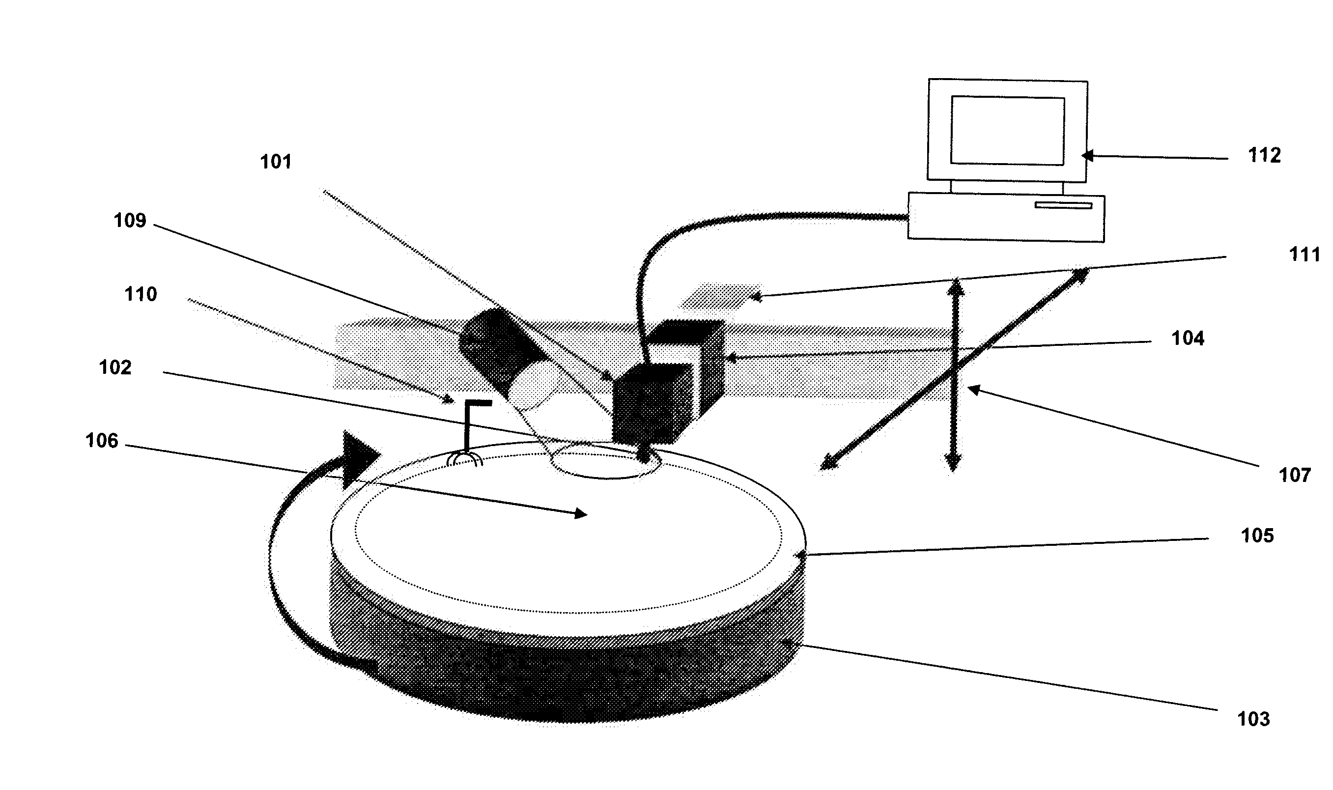
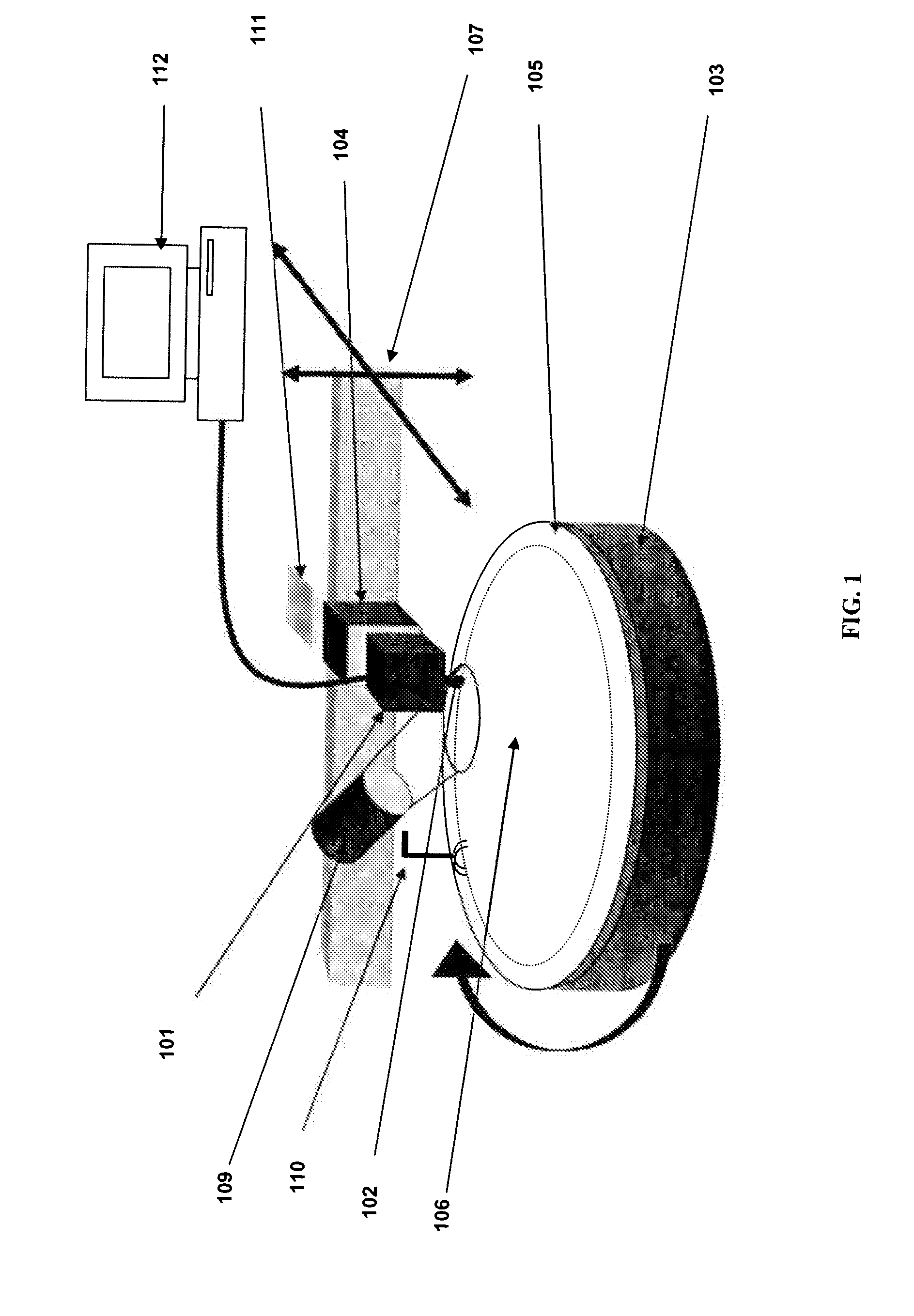
[0020]The average contact
potential difference between the probe tip and the wafer surface can be determined by making vibrating
Kelvin probe measurements at one or more points on the wafer surface. A bias
voltage which is equal in magnitude, but opposite in polarity, can then be applied to the probe tip to minimize the average difference in potential between the probe tip and wafer surface. The wafer can then be scanned using this bias
voltage, and the
signal component due to changes in the distance between the probe tip and the wafer surface will be minimized. Subsequent wafers with similar surfaces can also be scanned using the same bias
voltage without the need to make additional vibrating
Kelvin probe measurements. The use of a bias voltage which minimizes the average potential between the probe tip and the wafer surface permits the formation of a signal and image which can be used to identify non-uniformities in surface potential while minimizing the signal due to changes in the height.
[0021]One
advantage of the non-vibrating contact potential difference sensor is that it can acquire data relatively quickly, so that whole-wafer images can be acquired in only a few minutes. The availability of high-resolution images permits the use of
image processing algorithms to classify non-uniformities based on features associated with their shape or signal levels. For example, the differential or integrated image can be thresholded, and the resulting defect map can be segmented to identify connected regions of non-uniformity. Each region can then be associated with a
list of features; such as area, perimeter, height, width, signal range, average signal value, minimum and maximum signal values, and many others. These features can be calculated from the differential or integrated images of the non-uniformities, or from images acquired with different bias voltages, illumination configurations,
surface charge conditions, or combinations of these images. This
list of features can then be used to classify the defect based on a mathematical
algorithm or set of rules. For example, in the simplest case non-uniformities can be classified based on size or standard deviation of the non-vibrating contact potential difference sensor signal.
[0022]The ability to control the intensity,
wavelength, and angle of illumination; and the amount of charge on the wafer surface or embedded in
dielectric or other
layers present on the wafer provides additional methods of classifying defects or location and amounts of charge. The surface
potential change resulting from some types of defects is sensitive to surface illumination or charging. Illumination can be used to vary the surface potential by reducing the effect of electric fields in the semiconductor, while charge deposited or otherwise present on the surface, or in or on a
dielectric layer, can be used to induce electric fields and vary the distribution of charge within the semiconductor. The ability to control the illumination and
surface charge allows two or more scans to be acquired with different illumination and / or charge conditions. These scans can then be combined mathematically, for example by subtracting one scan image from another, to determine the change in signal due to changes in illumination or charge. Surface non-uniformities can then be classified based on the magnitude and polarity of the change in signal that results from changing illumination or changing
surface charge conditions.

