Shower plate electrode for plasma CVD reactor

a technology of plasma chemical vapor deposition and shower plate, which is applied in the field of shower plate electrodes, can solve the problems of increased amount of unwanted deposits that adhere to the walls of the reactor chamber, defects in processed substrates, and accumulation of unwanted deposits on the inner walls of the reaction chamber and on the surface of the susceptor, and achieve uniform cross-sectional area

Inactive Publication Date: 2009-06-18
ASM JAPAN
View PDF21 Cites 256 Cited by
  • Summary
  • Abstract
  • Description
  • Claims
  • Application Information

AI Technical Summary

Benefits of technology

[0012]Another aspect of the present application includes a plasma CVD apparatus having a plasma CVD reaction chamber. A susceptor for supporting a substrate is disposed inside the reaction chamber and configured to be used as a first electrode to generate a plasma. A shower plate used as a second electrode to generate the plasma faces the susceptor and has a plurality of holes extending through the shower plate, the holes each having a uniform cross-sectional area. A diameter of a smallest circular area of the shower plate having all of the holes is 0.95 to 1.05 times a diameter of largest possible substrate that can fit within a confining structure of the susceptor. The shower plate is electrically connected to one or more power sources.

Problems solved by technology

Products generated by a plasma chemical reaction in a reaction chamber during wafer processing result in unwanted deposits accumulating on inner walls of the reaction chamber and on the surface of the susceptor.
The deposits then adhere onto substrates as foreign objects and cause impurity contamination, which results in defects in processed substrates.
Due to the increasing size of the substrates, reaction chambers have also increased in capacity, resulting in an increase in the amount of unwanted deposits that adhere to reactor chamber walls.
Because of this increased cleaning time, the number of substrates processed per unit time (throughput) declines.

Method used


Image

  • Shower plate electrode for plasma CVD reactor
  • Shower plate electrode for plasma CVD reactor
  • Shower plate electrode for plasma CVD reactor

Examples


Embodiment Construction

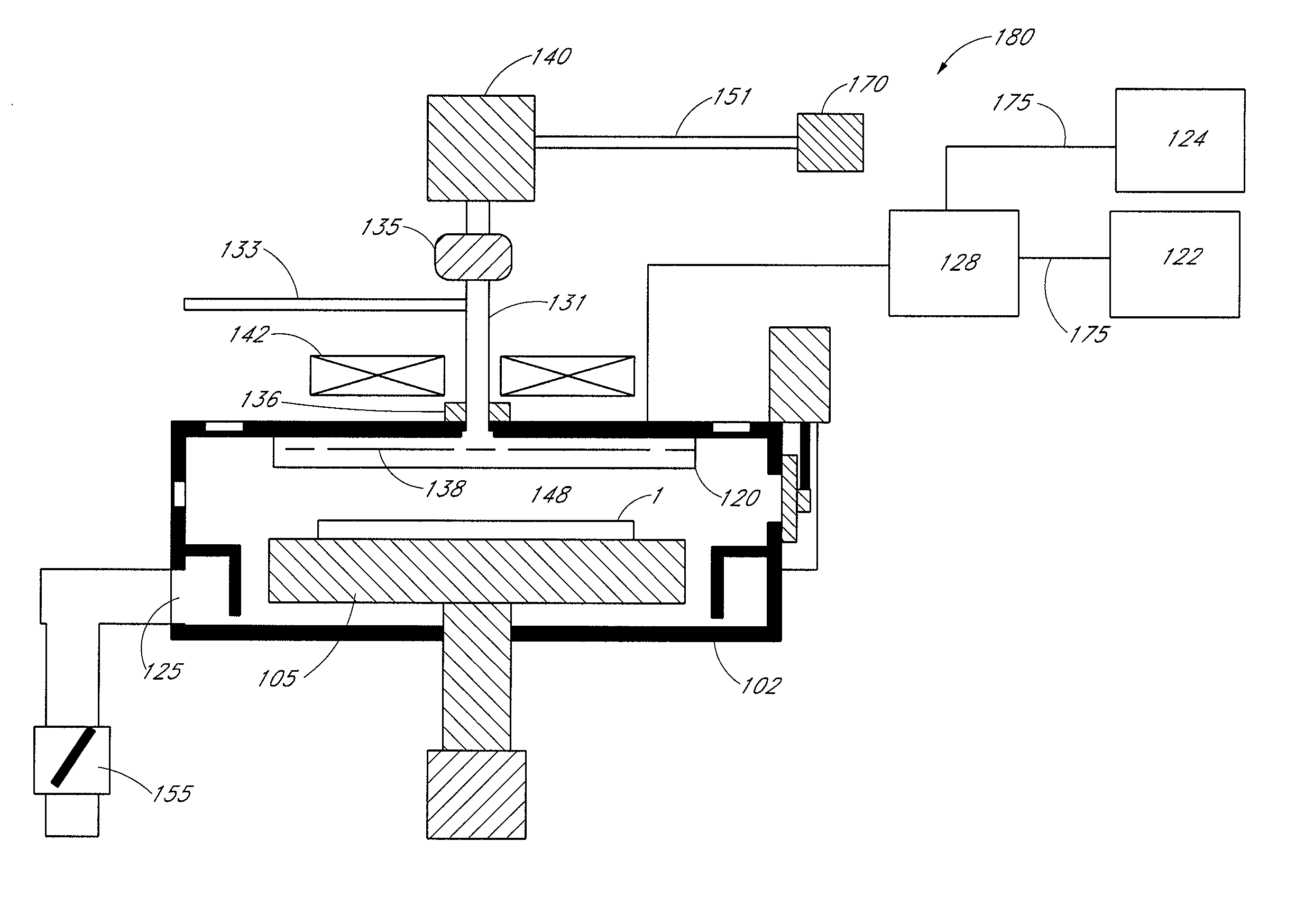
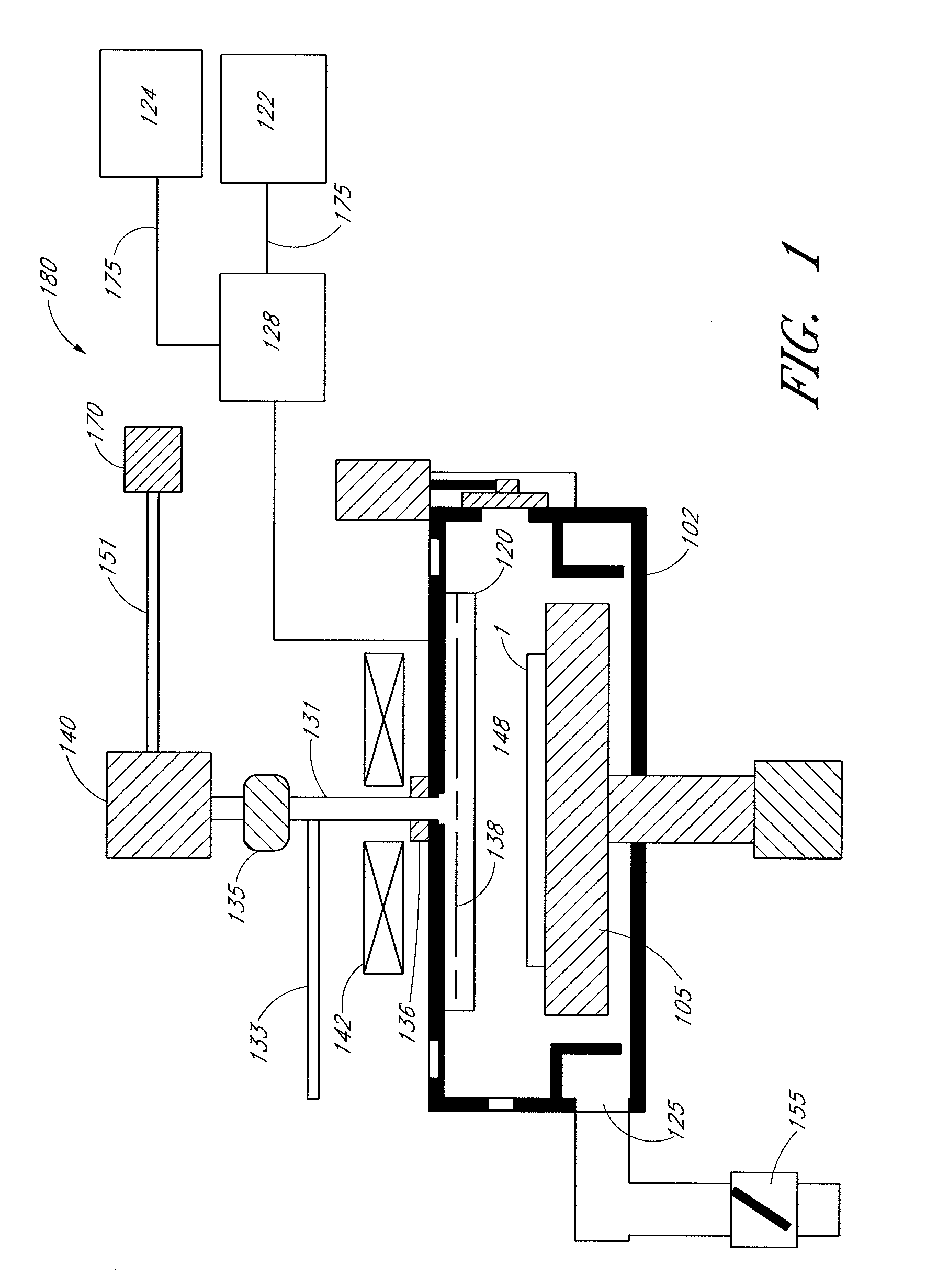
[0029]The present application relates to a plasma chemical vapor deposition (CVD) apparatus having a remote plasma generator for remote activation of a cleaning gas. More particularly, the application relates to a new shower plate having improved holes with a uniform cross-sectional area to improve the reactor cleaning rate in order to increase throughput.

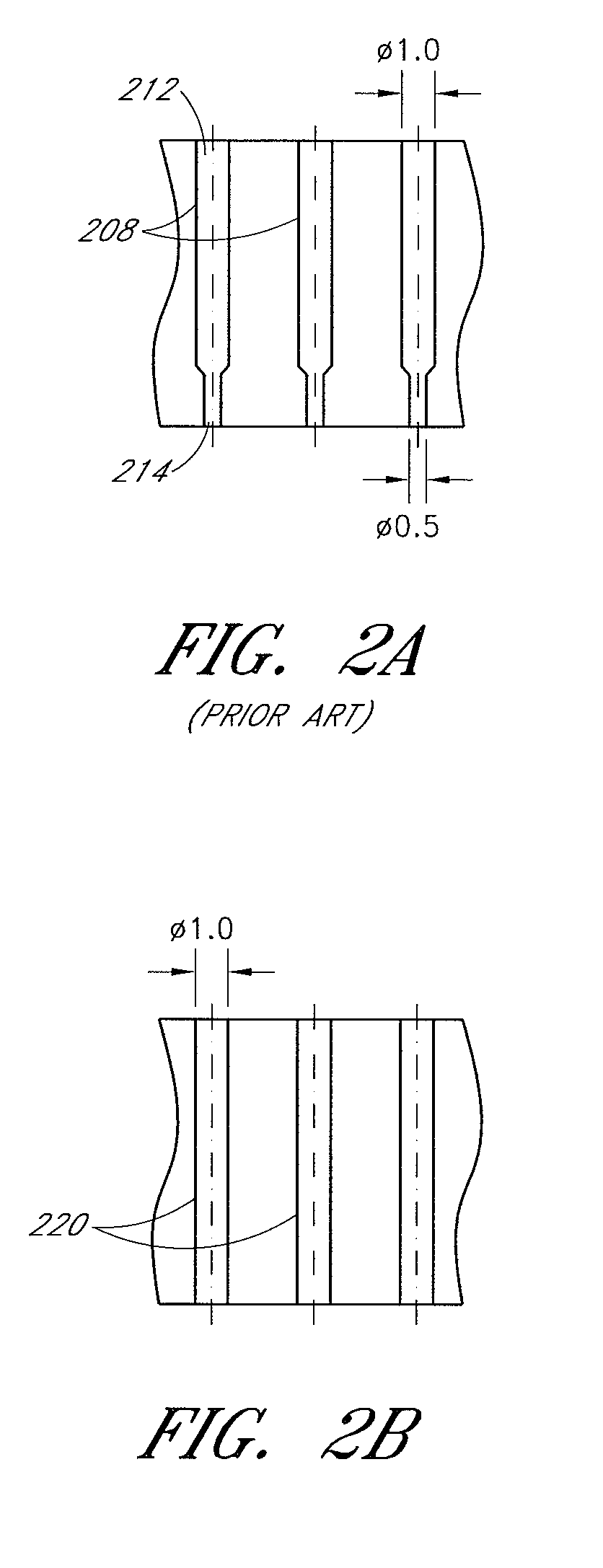
[0030]In a parallel-plate plasma CVD apparatus, the shower plate serves as an upper electrode for in situ plasma generation in reactant gases. By modifying the holes of the shower plate, including the dimensions of the holes, an improved reactor cleaning rate can be achieved. Moreover, careful selection of the size of the “hole machining area,” in conjunction with the modified holes, also leads unexpectedly to improved uniformity of films deposited during wafer processing, and in some cases an increased cleaning rate. As used herein, the hole machining area refers to the smallest circular area enclosing all of the holes of the show...


PUM

PropertyMeasurementUnit
diameteraaaaaaaaaa
diameteraaaaaaaaaa
diameteraaaaaaaaaa

Abstract

Methods and apparatuses for plasma chemical vapor deposition (CVD). In particular, a plasma CVD apparatus having a cleaning function, has an improved shower plate with holes having a uniform cross-sectional area to yield a high cleaning rate. The shower plate may serve as an electrode, and may have an electrically conductive extension connected to a power source. The shower plate, through which both cleaning gases and reaction source gases flow, may include a hole machined surface area with a size different than conventionally used to ensure a good film thickness uniformity during a deposition process. The size of the hole machined surface area may vary based on the size of a substrate to be processed, or the size of the entire surface of the shower plate.

Description

BACKGROUND OF THE INVENTION[0001]1. Field of the Invention[0002]The present invention relates to methods and apparatuses for plasma chemical vapor deposition (CVD). In particular, the present invention relates to shower plates.[0003]2. Description of the Related Art[0004]Generally, a plasma treatment apparatus is used for forming or removing films or for reforming the surface of an object-to-be-processed. In particular, thin film formation (by plasma CVD) on semiconductor wafers such as silicon or glass substrates or thin film etching is useful for manufacturing memories, semiconductor devices such as CPU's, or liquid crystal displays (LCDs).[0005]CVD apparatuses have been traditionally used for forming insulation films such as silicon oxide (SiO), silicon nitride (SiN), silicon carbide (SiC) and silicon oxide carbide (SiOC), as well as conductive films such as tungsten silicide (WSi), titanium nitride (TiN) and aluminum (Al) alloy on silicon or glass substrates. To form these films...

Claims


Application Information

Patent Timeline
Patent Type & Authority Applications(United States)
IPC IPC(8): C23C16/513B08B7/00
CPCC23C16/45565C23C16/505
Inventor NAKANO, RYUFUKUDA, HIDEAKI
Owner ASM JAPAN
Why Eureka
Try Eureka