

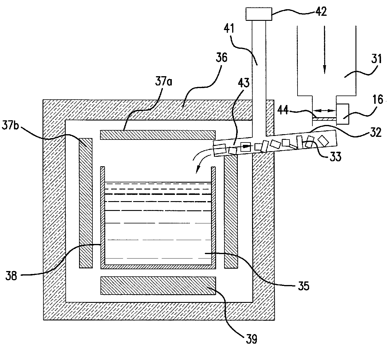
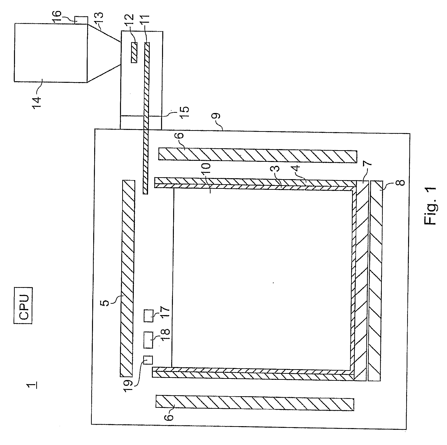
Method for producing a monocrystalline or polycrystalline semiconductore material
a monocrystalline or polycrystalline semiconductore and semiconductore technology, applied in the crystal growth process, from melt solutions, frozen solutions, etc., can solve the problems of complex measures, difficult to provide a suitably dimensionally stable annular attachment for reuse, and large volumetric shrinkage, so as to achieve short melting-on time, high filling level of the crucible, and uniform heating
- Summary
- Abstract
- Description
- Claims
- Application Information
AI Technical Summary
Benefits of technology
Problems solved by technology
Method used
Image

Examples
exemplary embodiment 1
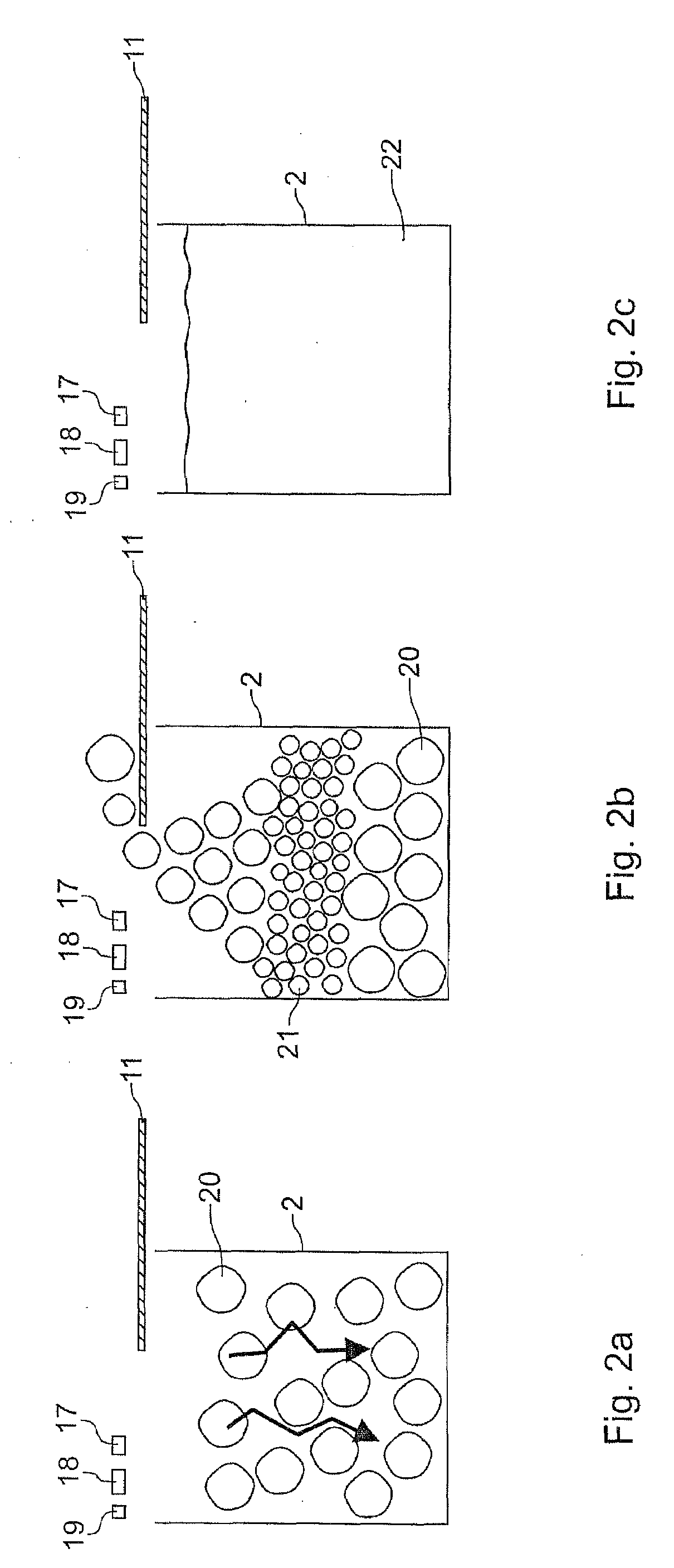
[0062]The surface temperature of the silicon feedstock in the melting crucible is continuously detected with the aid of a temperature sensor. It is thus possible to ascertain that and when the melting temperature of silicon is reached. Depending on the heating power for heating the melting crucible, the silicon feedstock slumps more or less rapidly. The silicon feedstock melts in this case from the surface. A predetermined time after reaching the melting temperature of silicon, additional silicon raw material is introduced into the melting crucible with the aid of the conveying means. The conveying rate is in this case adjusted in a suitable manner as a function of the actual heating power. The amount of silicon raw material that is actually introduced into the melting crucible is detected with the aid of the sensor. The silicon feedstock slumps continuously in the melting crucible. The additional silicon raw material can be introduced continuously or at predetermined intervals and ...
exemplary embodiment 2
[0063]The surface temperature of the silicon feedstock in the melting crucible is continuously detected with the aid of a temperature sensor. A central control means previously detected what amount of silicon feedstock has been introduced in the melting crucible. Or this amount can be input into the central control means. A predetermined amount of additional raw material is replenished to the melting crucible as a function of the current heating power and the amount of raw material currently located in the melting crucible. This replenishment can take place continuously or in a plurality of time-delayed steps at each of which a predefined amount of additional raw material is introduced. The additional silicon raw material is heated by the purposeful introduction of heat to a temperature just below the melting temperature of silicon, so that the melt in the melting crucible cools down only slightly and can quickly be brought back up to the prescribed operating temperature.
exemplary embodiment 3
[0064]A sensor is used continuously to detect the surface temperature of the crucible filling and therefore to determine the point in time at which the melting temperature of silicon is reached. A predetermined time after reaching the melting point, a predetermined amount of additional raw material is replenished to the melting crucible as a function of the actual heating power. This step is repeated after predetermined time intervals, in accordance with the current heating power, until a predetermined filling level of the melting crucible is reached. The additional silicon raw material is heated by the purposeful introduction of heat to a temperature just below the melting temperature of silicon, so that the melt in the melting crucible cools down only slightly and can quickly be brought back up to the prescribed operating temperature.
PUM
| Property | Measurement | Unit |
|---|---|---|
| temperature | aaaaa | aaaaa |
| area | aaaaa | aaaaa |
| volumetric shrinkage | aaaaa | aaaaa |
Abstract
Description
Claims
Application Information