Method of Growing Nitride Semiconductor material

a technology of nitride and semiconductors, applied in the direction of semiconductor devices, basic electric elements, electrical equipment, etc., can solve the problems of poor internal quantum efficiency, low crystalline quality, and low external quantum efficiencies of ingan green leds, so as to reduce the density of v-defects, increase yield, and increase flatness

Inactive Publication Date: 2009-06-25
NAT CENT UNIV
View PDF5 Cites 22 Cited by
  • Summary
  • Abstract
  • Description
  • Claims
  • Application Information

AI Technical Summary

Benefits of technology

[0006]It is therefore one object of the invention to provide a method of growing nitride semiconductor material for a plurality of semiconductor devices, the method comprising flowing Triethyl-gallium (TEGa) and ammonia (NH3) into a chamber to grow a first barrier layer; flowing Trimethyl-indium (TMIn) into the chamber to grow a first well layer; stopping flowing TEGa to grow an InN treatment layer in the chamber; stopping flowing TMIn; flowing TEGa into the chamber to grow a second barrier layer; and forming an InN-based LED of multiquantum well (MQW). The method can be applied to the manufacturing of InN MQW LED, InN quantum dots LED structure, rectifier, HBT, or HEMT. By utilizing this method, advantages including increased flatness, decreased density of V-defects, increased yield and increased light emission efficiency of LEDs made of a material including the nitride semiconductor material can be obtained.

Problems solved by technology

However, the external quantum efficiencies (EQE) of InGaN green LEDs still falls short of what is required.
Poor internal quantum efficiency has been identified to be the bottleneck and has become the focus of intensive studies recently.
The fundamental issue of this task is to obtain high quality InxGa1-xN alloys at a high indium mole fraction, which often leads to low crystalline quality due to indium aggregation and / or phase separation.
Furthermore, V-defects are the most common defect that occurs at InGaN / GaN quantum wells of high indium mole fraction.
Previous works have demonstrated that the V-shape defects are easily formed in high indium MQW, not only from buffer layer treading dislocations, but also within the MQW because of strain relaxation associated with stacking faults or indium segregation.

Method used


Image

  • Method of Growing Nitride Semiconductor material
  • Method of Growing Nitride Semiconductor material
  • Method of Growing Nitride Semiconductor material

Examples


Embodiment Construction

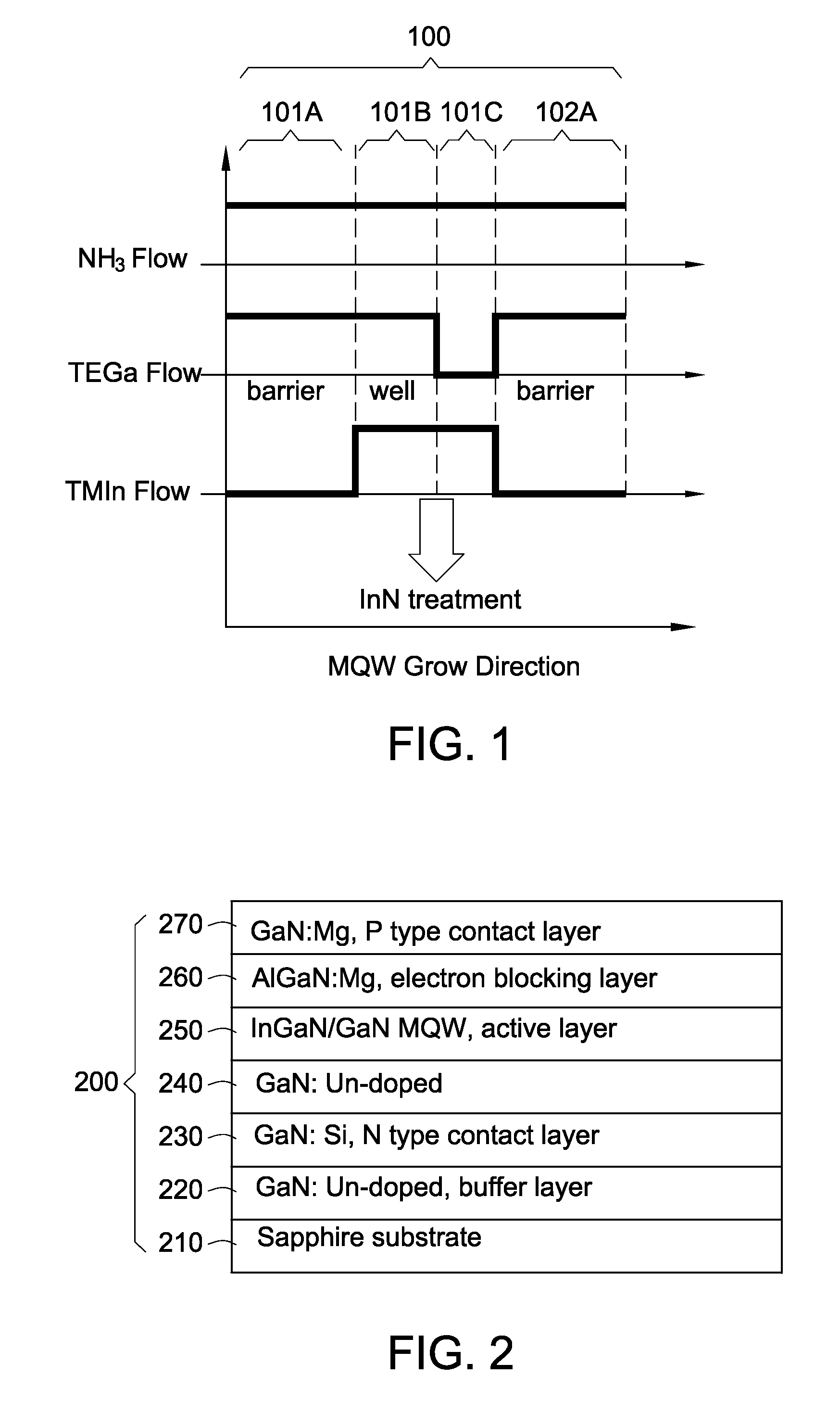
[0019]Referring to FIG. 1, it is a graph showing multiquantum well (MQW) growth direction versus different flows for InN treatment active layer 100 manufactured according to a method of growing nitride semiconductor material of the invention. The method comprises the following steps.

[0020]First, flow Triethyl-gallium (TEGa) and ammonia (NH3) into a chamber to grow a first barrier layer 101A.

[0021]Next, flow Trimethyl-indium (TMIn) into the same chamber to grow a first well layer 101B.

[0022]Next, stop flowing TEGa to grow an InN treatment layer 101C in the chamber. Next, stop flowing TMIn and flow TEGa into the chamber again to grow a second barrier layer 102A.

[0023]Finally, an InN treatment LED of MQW is produced. The LED has a flat MQW structure with decreased density of V-defects and increased light emission efficiency.

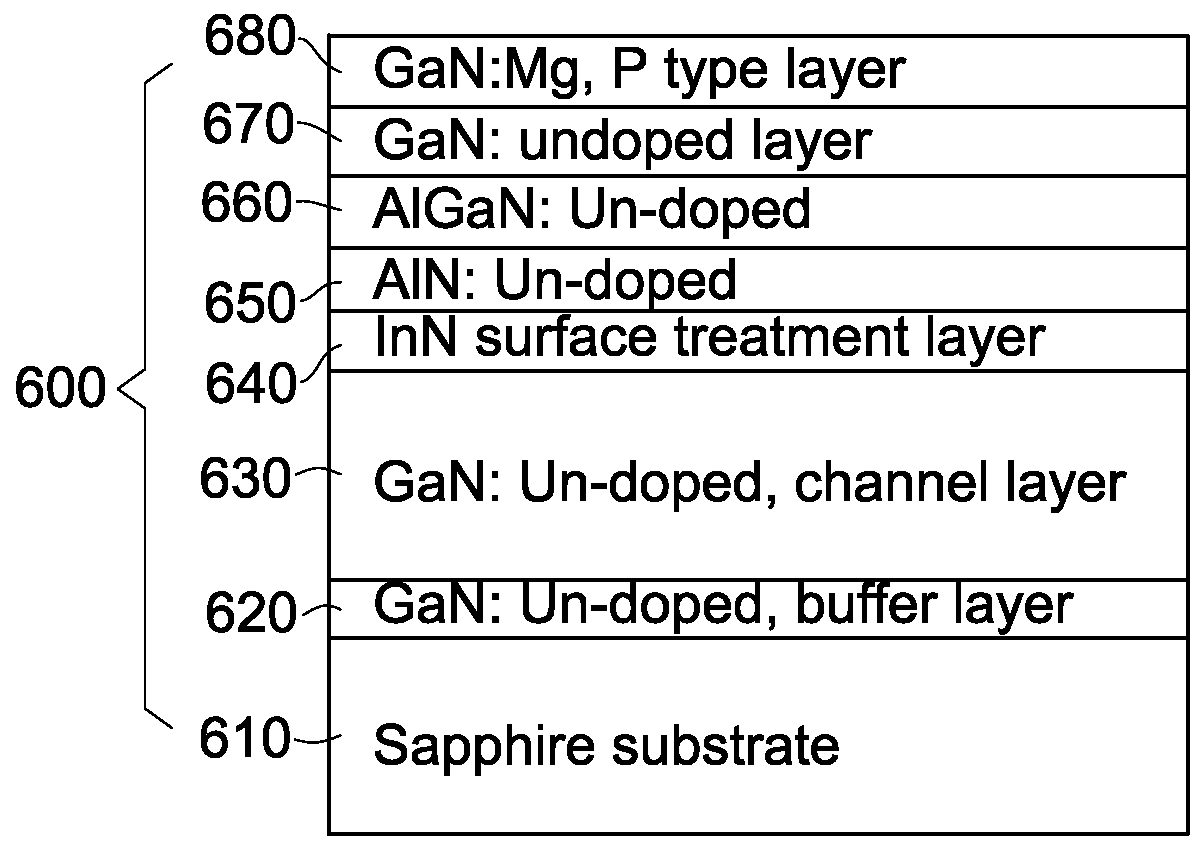
[0024]Referring to FIG. 2, it is a sectional view showing the constituent layers of an InN treatment MQW LED structure 200 manufactured according to the method of t...


PUM

PropertyMeasurementUnit
semiconductoraaaaaaaaaa
flatnessaaaaaaaaaa
densityaaaaaaaaaa

Abstract

A method of growing nitride semiconductor material and particularly a method of growing Indium nitride is disclosed can increase surface flatness of a nitride semiconductor material and decrease density of V-defects therein. Further, the method can increase light emission efficiency of a quantum well or quantum dots of the produced LED as well as greatly increase yield. The method is also applicable to the fabrications of electronic devices made of nitride semiconductor material and diodes of high breakdown voltage for rectification. The method can greatly increase surface flatness of semiconductor material for HBT, thereby increasing quality of the produced semiconductor devices.

Description

BACKGROUND OF THE INVENTION[0001]1. Field of Invention[0002]The invention relates to methods of growing nitride semiconductor material and more particularly to such a method of growing nitride semiconductor material with improved characteristics including increased flatness and decreased density of V-defects, thereby increasing yield and increasing light emission efficiency of LEDs (light-emitting diodes) made of a material including the nitride semiconductor material.[0003]2. Description of Related Art[0004]The rapid advances in light-emitting diodes (LEDs) have led to the advent of the solid-state lighting era for reduced consumption of natural resources. InGaN alloy is the most promising material for high-efficiency light sources because of its direct band gap nature and widely spanned emission spectrum from ultraviolet to infrared. Moreover, the excellent properties of GaN-based materials such as high temperature stability, high breakdown voltage, high electron velocity, strong ...

Claims


Application Information

Patent Timeline
Patent Type & Authority Applications(United States)
IPC IPC(8): H01L21/36
CPCH01L21/0242H01L21/02458H01L33/06H01L21/0262H01L33/0062H01L21/0254
Inventor LIN, HUNG-CHENGCHYI, JEN-INN
Owner NAT CENT UNIV
Why Eureka
Try Eureka