Method of forming high-dielectric constant films for semiconductor devices

a technology of dielectric constant and semiconductor devices, applied in the direction of vacuum evaporation coating, chemical vapor deposition coating, coating, etc., can solve the problems of large densities of interface traps, many high-k materials under evaluation suffer from various problems, and no longer function as effective gate insulators, etc., to achieve good thickness uniformity, improve material and electrical properties of the film, and effectively remove carbon and other impurities

Active Publication Date: 2009-06-25
TOKYO ELECTRON LTD
View PDF22 Cites 67 Cited by
  • Summary
  • Abstract
  • Description
  • Claims
  • Application Information

AI Technical Summary

Benefits of technology

[0004]A method is provided for forming high dielectric constant (high-k) films for semiconductor devices using a film deposition sequence that includes exposing a substrate to temporally separated and alternating reactant pulses. According to one embodiment, the substrate is maintained at a temperature suitable for atomic layer deposition (ALD). According to another embodiment, the substrate can be maintained at a temperature below which is suitable for ALD. The method is capable of forming a high-k film with good thickness uniformity while impeding growth of an interface layer between the high-k film and the substrate. According to embodiments of the invention, the deposited high-k film may be treated with an oxidation process to improve the material and electrical properties of the film.
[0005]According to one embodiment of the invention, a method is provided for forming a metal-carbon-oxygen high-k film for a semiconductor device. The method includes disposing a substrate in a process chamber and providing a film deposition sequence of a first reactan

Problems solved by technology

In microelectronics, continuous shrinking of devices is necessary to improve the performance, which sets challenging requirements for fabrication of integrated circuits (ICs).
High-k materials have been extensively studied due to the fact that SiO2, which is traditionally used as a gate oxide in metal-oxide semiconductor field effect transistors (MOSFETs), can no longer function as an effective gate insulator as higher capacitance density with decreased gate oxide thickness is required for near-future device gene

Method used


Image

  • Method of forming high-dielectric constant films for semiconductor devices
  • Method of forming high-dielectric constant films for semiconductor devices
  • Method of forming high-dielectric constant films for semiconductor devices

Examples


Embodiment Construction

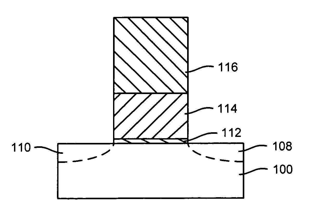
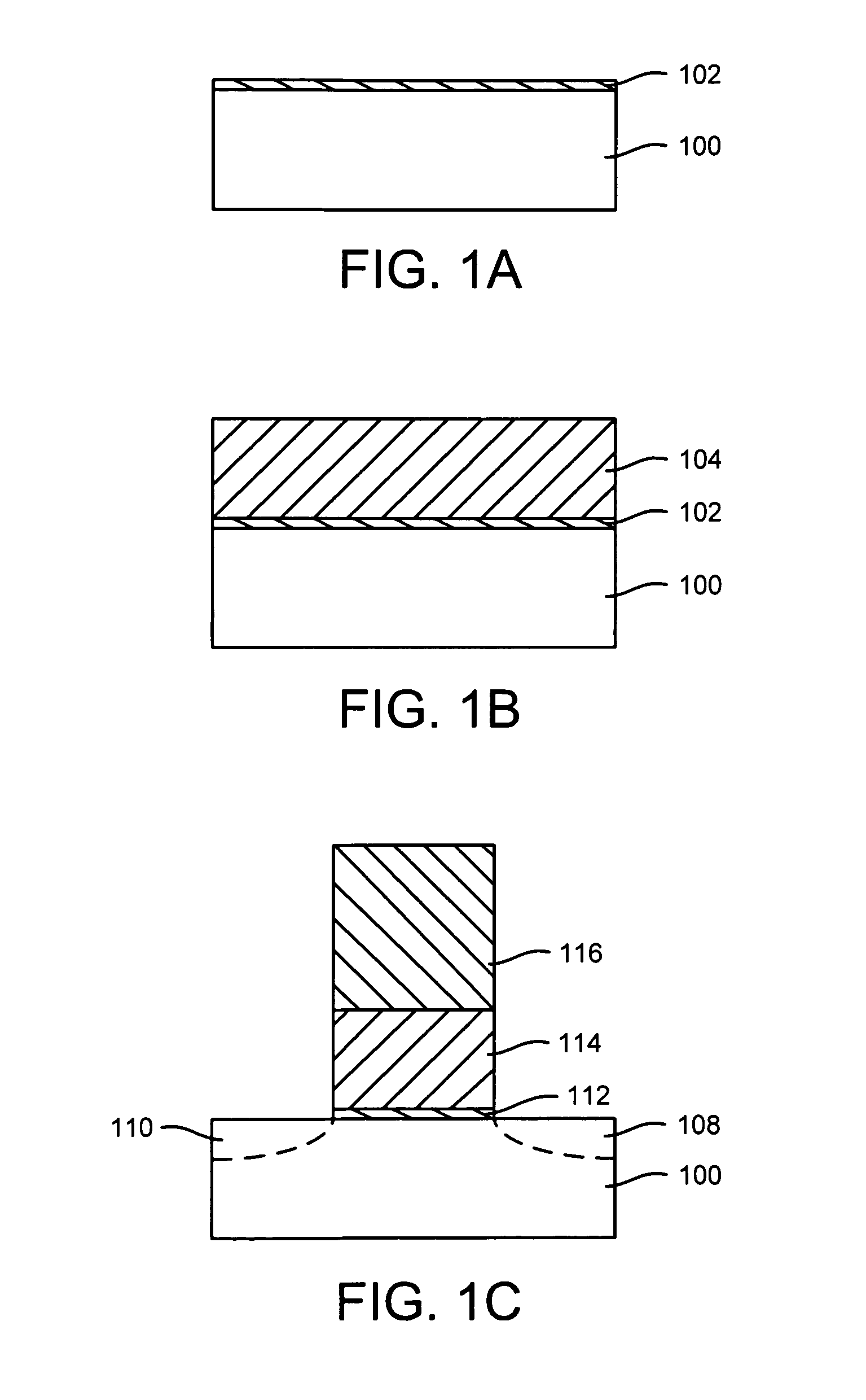
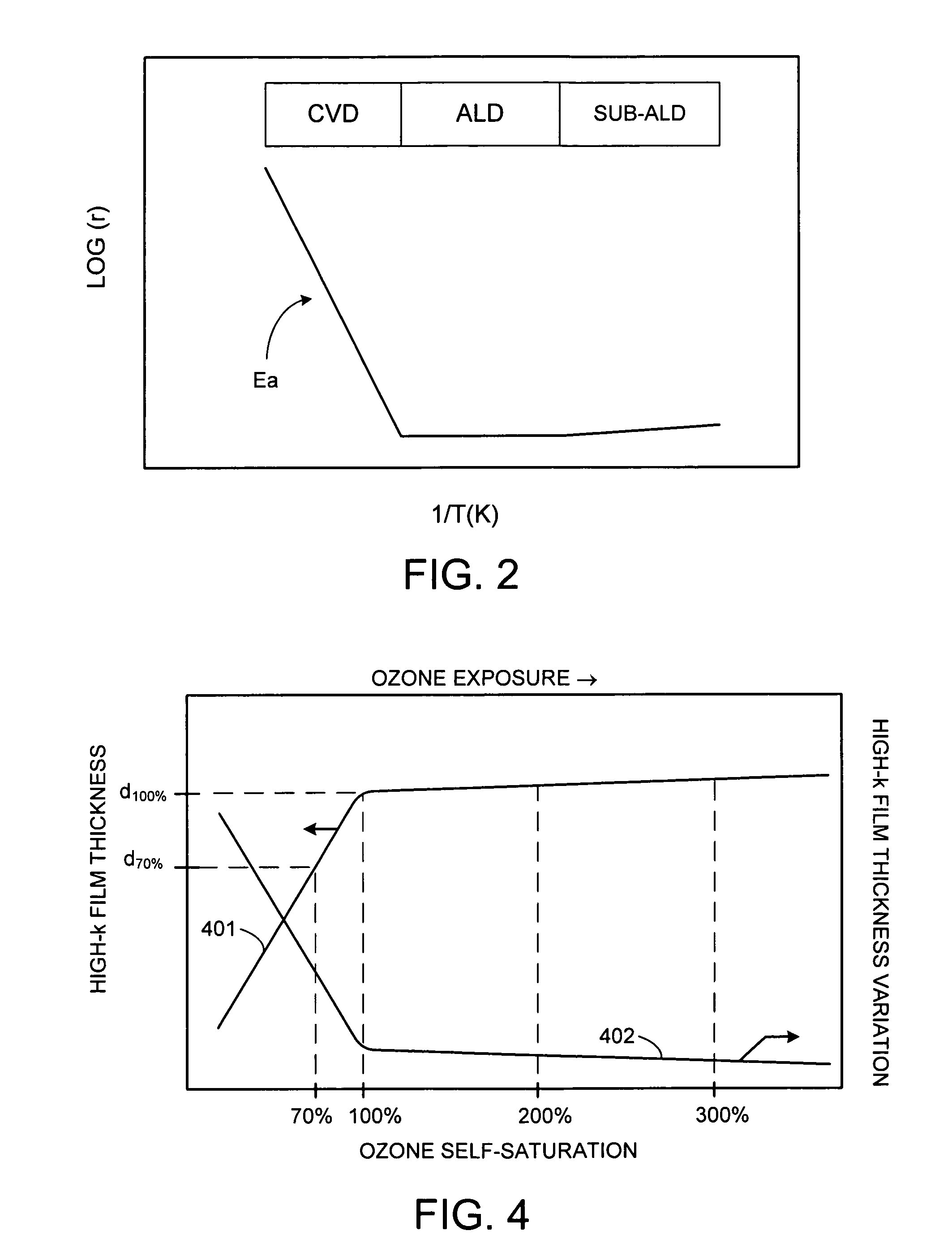
[0016]Methods for depositing high-k films for semiconductor devices using a film deposition sequence that include exposing a substrate to temporally separated and alternating reactant pulses is described in various embodiments. One skilled in the relevant art will recognize that the various embodiments may be practiced without one or more of the specific details, or with other replacement and / or additional methods, materials, or components. In other instances, well-known structures, materials, or operations are not shown or described in detail to avoid obscuring aspects of various embodiments of the invention. Similarly, for purposes of explanation, specific numbers, materials, and configurations are set forth in order to provide a thorough understanding of the invention. Furthermore, it is understood that the various embodiments shown in the figures are illustrative representations and are not necessarily drawn to scale.

[0017]Reference throughout this specification to “one embodime...


PUM

PropertyMeasurementUnit
Fractionaaaaaaaaaa
Fractionaaaaaaaaaa
Temperatureaaaaaaaaaa

Abstract

A method is provided for forming high dielectric constant (high-k) films for semiconductor devices. According to one embodiment, a metal-carbon-oxygen high-k film is deposited by alternately and sequentially exposing a substrate to a metal-carbon precursor and near saturation exposure level of an oxidation source containing ozone. The method is capable of forming a metal-carbon-oxygen high-k film with good thickness uniformity while impeding growth of an interface layer between the metal-carbon-oxygen high-k film and the substrate. According to one embodiment, the metal-carbon-oxygen high-k film may be treated with an oxidation process to remove carbon from the film.

Description

FIELD OF INVENTION[0001]The present invention relates generally to the field of forming high dielectric constant (high-k) films for semiconductor devices and more particularly to methods for forming high-k films with good thickness uniformity on substrates while impeding oxidation of the substrates.BACKGROUND OF THE INVENTION[0002]In microelectronics, continuous shrinking of devices is necessary to improve the performance, which sets challenging requirements for fabrication of integrated circuits (ICs). New manufacturing techniques are required for growing very thin blanket films and thin films covering deep trenches and other three dimensional (3D) structures with good conformality. Atomic layer deposition (ALD) has gathered interest in the microelectronic industry from the unique characteristics that the method offers: ultra-thin films can be deposited on large substrates with excellent conformality and with control of thickness and composition at the nanometer level. ALD has high...

Claims


Application Information

Patent Timeline
IPC IPC(8): H01L21/28H01L21/31
CPCC23C16/30C23C16/40C23C16/45529C23C16/45531H01L21/28167H01L29/517H01L21/3141H01L21/31641H01L21/31645H01L29/495H01L29/4966H01L21/28194H01L21/02205H01L21/0228H01L21/02175H01L21/02337
Inventor CLARK, ROBERT D.WAJDA, CORY
Owner TOKYO ELECTRON LTD
Why Eureka
Try Eureka