

Wiring Boards and Processes for Manufacturing the Same
a technology of wiring boards and manufacturing processes, applied in the field of wiring boards, can solve the problems of reducing the bonding reliability of an inner lead and an electronic component mounted thereon, increasing conductor resistance, and causing frequent conduction failures, etc., to reduce the electrical resistance of excessive etching of wires, and reduce the number of etched wires. , the effect of small cross sectional area
- Summary
- Abstract
- Description
- Claims
- Application Information
AI Technical Summary
Benefits of technology
Problems solved by technology
Method used
Image

Examples
example 1
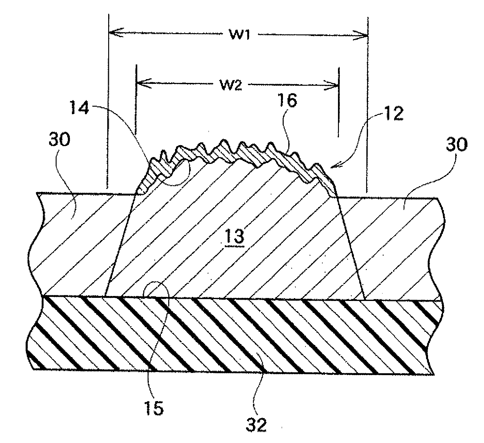
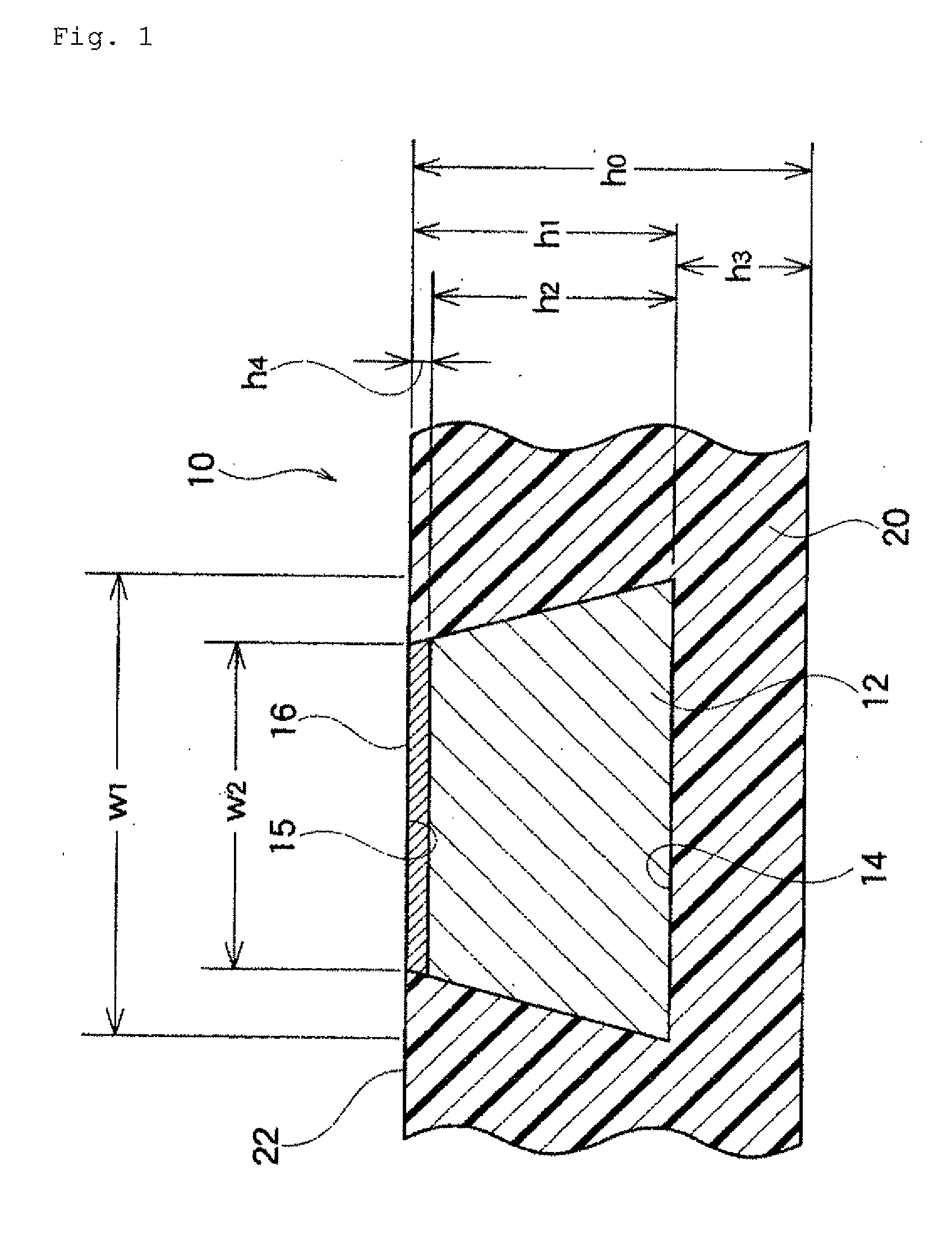
[0173]A support electrodeposited copper foil 48 mm in width and 35 μm in thickness (VLP copper foil manufactured by MITSUI MINING & SMELTING CO., LTD.) was roll coated with a positive typed photoresist (FR200-8CP manufactured by Rohm and Hass Company) to a thickness of 6 μm. The photoresist was dried and cured at 100° C. for 1 minute, and was exposed with an exposure apparatus to draw a pattern at 20 μm pitches.
[0174]The exposure apparatus was EP-70SAC-02 (manufactured by USHIO INC., light intensity: 64 mW / cm2) capable of emitting energy beams with dominant wavelengths of 365 nm, 405 nm and 436 nm. The energy density was 630 mJ / cm2. The resist was developed by being soaked in a 1.5% KOH solution for 65 seconds. The bottom opening and the top opening were 6.9 μm and 12.2 μm in width respectively.
[0175]Electroplating was performed for 1 minute using a gold plating solution (TEMPEREX 8400 manufactured by EEJA) at 65° C. and Dk of 0.2 A / dm2, resulting in a 0.1 μm thick gold deposit laye...
example 2
[0184]A support electrodeposited copper foil 70 mm in width and 35 μm in thickness (VLP copper foil manufactured by MITSUI MINING & SMELTING CO., LTD.) was roll coated with a positive typed photoresist (FR200-8CP manufactured by Rohm and Hass Company) to a thickness of 6.8 μm. The photoresist was dried and cured at 100° C. for 1 minute, and was exposed with an exposure apparatus to draw a pattern at 20 μm pitches.
[0185]The exposure apparatus was EP-70SAC-02 (manufactured by USHIO INC., light intensity: 64 mW / cm2) capable of emitting energy beams with dominant wavelengths of 365 nm, 405 nm and 436 nm. The energy density was 630 mJ / cm2. The resist was developed by being soaked in a 1.5% KOH solution for 65 seconds. The bottom opening and the top opening were 6.2 μm and 11.5 μm in width respectively.
[0186]Electroplating was performed for 1 minute using a gold plating solution (TEMPEREX 8400 manufactured by EEJA) at 65° C. and Dk of 0.2 A / dm2, resulting in a 0.1 μm thick gold deposit la...
example 3
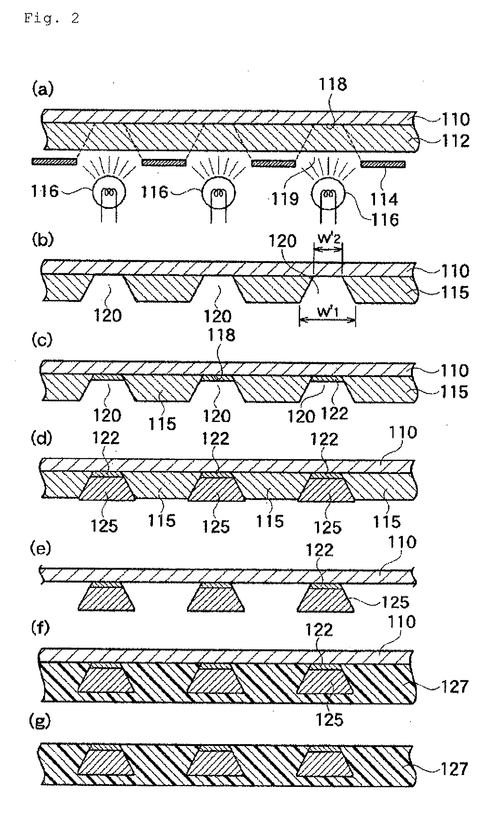
[0196]An electrodeposited copper foil 3 μm in thickness (MicroThin copper foil manufactured by MITSUI MINING & SMELTING CO., LTD.) was laminated to an adhesive-coated PET film 48 mm in width and 50 μm in thickness. To the resultant two-layer laminate film, an etching solution having a temperature of 40° C. was sprayed for 20 seconds from nozzles located 15 cm above the laminate film. Consequently, the copper foil was etched to a thickness of 1 μm. The etching solution used herein had a hydrochloric acid concentration of 85.4 to 87.6 g / l, a Cu ion concentration of 115 to 135 g / l, and a specific gravity of 1.250 to 1.253. The etching solution was sprayed from two nozzles at a pressure of 2 kg / cm2 and a flow rate of 1.83 l / min per nozzle.
[0197]The half-etched copper foil was roll coated with a positive typed photoresist (FR200-8CP manufactured by Rohm and Hass Company) to a thickness of 6.5 μm. The photoresist was dried and cured at 100° C. for 1 minute, and was exposed with an exposur...
PUM
| Property | Measurement | Unit |
|---|---|---|
| thickness | aaaaa | aaaaa |
| thickness | aaaaa | aaaaa |
| width | aaaaa | aaaaa |
Abstract
Description
Claims
Application Information