Method and Apparatus for Manufacture of Via Disk

a technology of via disk and manufacturing method, which is applied in the manufacture of cables/conductors, instruments, coatings, etc., can solve the problems of inability to maintain sufficient planarity and surface parallelism, difficulty in maintaining electrical continuity and supporting high-performance signals, and multi-layer substrates using cast ceramics or “green tapes”. achieve good planarity, maintain dimensional control, and ensure the effect of continuity

Active Publication Date: 2009-07-30
INNOVENT TECH
View PDF48 Cites 6 Cited by
  • Summary
  • Abstract
  • Description
  • Claims
  • Application Information

AI Technical Summary

Benefits of technology

[0011]In order to alleviate the disadvantages associated with the shrinkage that accompanies tape cast ceramic manufacture or the non-conductive “open” vias in hardened ceramics using molybdenum or tungsten inks, the use of hardened materials such as ceramics (e.g. alumina, aluminum nitride, etc.) or glass composites (e.g. Pyrex, etc.) are presented together with a method that fills vias with a minimum of voiding or other electrical discontinuity even as via length increases. Because hardened ceramics are rigid and stable, their ability to scale to larger size (wafer-scale) while maintaining dimensional control, good planarity, and surface finish, present significant benefits. Further, hardened ceramics can be obtained in higher purities than cast ceramics, providing for additional improvement in electrical performance. The invention uses a pressurized metal infiltration process to ensure each via is properly filled and avoids the shrinkage issues, open vias, low yields, and high costs associated with cofired and other conventional techniques.

Problems solved by technology

One problem associated with these techniques is an inability to maintain sufficient planarity and surface parallelism as dimensions increase beyond 4-6 inches in length or width.
In addition, as thickness increases, vertical routing requires the use of multiple dielectric layers and the maintenance of electrical continuity and support of high performance signals becomes a challenge.
However, the manufacture of multi-layer substrates using cast ceramic, or “green tape,” introduces its own problems.
This technology possesses a number of disadvantages due to potential variation in the alignment of conductive patterns, vias and cavities which limit interconnect density.
These problems are created by the differential shrinkage within and between the individual layers of the ceramic material from which the multi-layer substrate is formed.
Also, the surface roughness of the tape cast ceramics limit electrical performance.
Further, since tape cast or green sheet ceramics can contain between 8% and 40% binders, the purity levels of the processed ceramics are not tightly controlled, leading to a compromise in electrical performance.
In addition, the intrinsic shrinkage of the tape cast ceramic impacts the filling of vias such that voiding and / or other discontinuities become more challenging as the thickness of the substrate increases.
However, this process may leave a significant number of electrically non-conductive “open” vias that render them unusable.
Due to the above-described problems, via disks manufactured using co-fired technology have very low yields, often not exceeding 25%.
These low yields result in long lead times, as well as increased costs.

Method used


Image

  • Method and Apparatus for Manufacture of Via Disk
  • Method and Apparatus for Manufacture of Via Disk
  • Method and Apparatus for Manufacture of Via Disk

Examples


example

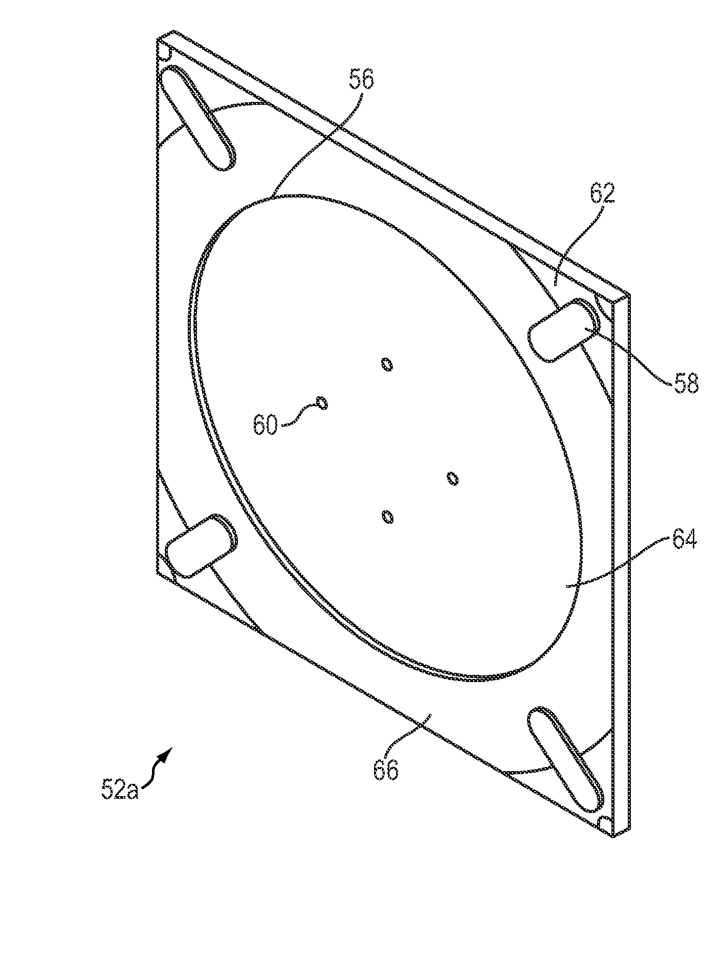
[0044]A Ø 100 mm AVD was manufactured in accordance with the teachings herein, specifically, a drilled ceramic disk was placed in a mold and heated to about 700° C. and pressurized with A356.2 aluminum alloy infiltrant to a pressure of about 1000 psi for approximately 30 minutes. The mold was then allowed to cool at ambient pressure until it reached ambient temperature. After processing to remove excess material, various tests were performed to determine performance characteristics of the AVD. The results of these tests are presented below.

[0045]Since the via forms part of the signal path, it is generally desirable that the via displays a low resistance value. To test resistance of the filled vias, five vias were chosen for measurement at various locations on the prepared sample. Resistance was measured at both 1 and 5 volts. The results are depicted in Table 1, below.

TABLE 1Via Resistance Test ResultsTest PointSourceSourceMeterResultsNo.Set VoltCurrentmilliVoltsΩ× 10−3150.10.1251.2...


PUM

PropertyMeasurementUnit
diameteraaaaaaaaaa
diameteraaaaaaaaaa
diameteraaaaaaaaaa

Abstract

Aluminum filled via disks are manufactured utilizing a plurality of drilled substrates placed into a metal can in a stacked, interdisposed assembly with a corresponding number of graphite molds. Aluminum infiltration ingots are added and the can is heated to a temperature to melt the ingots. The molten aluminum is pressurized so that it flows into the vias. The substrates are then cooled, removed from the can, separated from between the graphite molds, and the flat surface faces are ground and polished to expose the filled vias.

Description

CROSS REFERENCE TO RELATED APPLICATION[0001]This application claims priority under 35 U.S.C. § 119(e) to U.S. Provisional Patent Application Ser. No. 61 / 024,708, filed Jan. 30, 2008, the disclosure of which is hereby incorporated by reference herein in its entirety.BACKGROUND OF THE INVENTION[0002]A ceramic via disk is a circular alumina substrate that includes a large number of closely spaced, precisely located holes or vias formed therethrough. These vias are filled with conductive material to provide isolated conductive regions through the insulating ceramic substrate. The disk can be scaled to match the size of a semiconductor wafer.[0003]Ceramic via disks are well-suited for probe card applications, specifically to facilitate space transformation. The probe card is a custom-designed interface that provides electrical signal paths between the test system and circuits on a wafer, thereby permitting the testing and validation of the circuits at wafer level, before the wafers are c...

Claims


Application Information

Patent Timeline
Patent Type & Authority Applications(United States)
IPC IPC(8): H05K1/11B05D5/12B29C63/26
CPCG01R1/07378H01L23/49827H05K1/0306H05K3/101Y10T29/49165H05K2203/128H01L2924/0002H05K3/4038H01L2924/00
Inventor VAN DEN HOEK, WILLIBRORDUS G.KILKELLY, MICHAEL J.FAWKES, DANETWAALFHOVEN, FELIXKILKELLY, BARBARA
Owner INNOVENT TECH
Why Eureka
Try Eureka