Method of manufacturing a semiconductor device

a manufacturing method and technology of semiconductor devices, applied in the direction of basic electric elements, radiation controlled devices, transistors, etc., can solve the problems of difficult stably carrying out the first thermal treatment to form, the aggregation of ni and si, and the inability to achieve high-speed operation, so as to reduce the variation of electrical characteristics of metal silicide layers and improve throughput. , the effect of improving the reliability and product yield of semiconductor elements

Active Publication Date: 2009-07-30
RENESAS ELECTRONICS CORP
View PDF8 Cites 27 Cited by
  • Summary
  • Abstract
  • Description
  • Claims
  • Application Information

AI Technical Summary

Benefits of technology

[0031]The present embodiment is a method of manufacturing a semiconductor device for forming a silicide layer with a low resistance over the surface of a gate electrode and a source/drain region of a field effect transistor by a self-alignment method. The method, first, after forming a gate insulating film, a gate electrode, and a source/drain region of a field effect transistor over a semiconductor substrate made of single crystal silicon, forms an alloy film of nickel and platinum over the semiconductor substrate. The method then, by carrying out a first thermal treatment at a thermal treatment temperature of 210 to 310° C. using a heater heating device, causes the alloy film and silicon constituting the gate electrode or source/drain region to react with each other to form a platinum-added nickel silicide layer in a (PtNi)2Si phase, then after removing the unreacted alloy film, by carrying out a second thermal treatment at a thermal treatment temperature higher than that of the first thermal treatment, forms a platinum-added nickel silicide layer in a PtNiSi phase. The temperature rise rate of the first thermal treatment is set to 10° C./s or more (for example, 30 to 250° C./s) and the temperature rise rate of the second thermal treatment is set to 10° C./s or more (for example, 10 to 250° C./s).
[0032]The present embodiment is a method of manufacturing a semiconductor device for forming a silicide layer with a low resistance over the surface of a gate electrode and a source/drain region of a field effect transistor by a self-alignment method. The method, first, after forming a gate insulating film, a gate electrode, and a source/drain region of a field effect transistor over a semiconductor substrate made of single crystal silicon, forms an alloy film of nickel and platinum over the semiconductor substrate. The method then, by carrying out a first thermal treatment at a thermal treatment temperature of 380 to 400° C. using a heater heating device, causes the alloy film and silicon constituting the gate electrode or source/drain region to react with each other to f...

Problems solved by technology

With the progress of high integration of a semiconductor device, a field effect transistor is miniaturized in accordance with the scaling law, however, there arises a problem that a high-speed operation cannot be obtained even if the field effect transistor is miniaturized because the resistance of a gate, source, and drain increases.
However, about the nickel silicide layer formed by the SALICIDE technique, there are various technical problems to be described below.
That is, it has been revealed that there are many defects on the surface of the nickel silicide layer in the NiSi phase formed by the thermal treatment in the two stages described above and variations in electrical characteristics are caused.
This may result from aggregation of Ni and Si due to the application of an excessive amount of heat to the wafer in the second thermal treatment carried out to stabilize the NiSi phase.
Further, before an insulating film is formed over the nickel silicide layer, the surface of the nickel silicide layer is subjected to the plasma cleaning process and the change in composition of NiSi due to the plasma cleaning process is one of the causes...

Method used


Image

  • Method of manufacturing a semiconductor device
  • Method of manufacturing a semiconductor device
  • Method of manufacturing a semiconductor device

Examples


first embodiment

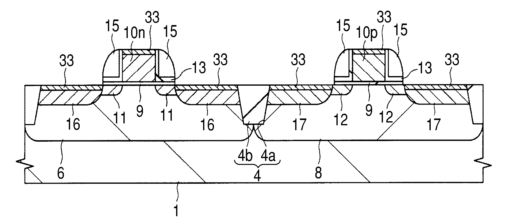
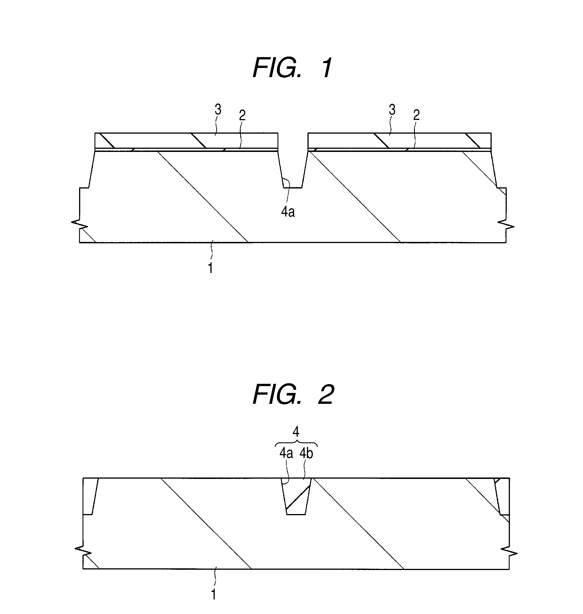
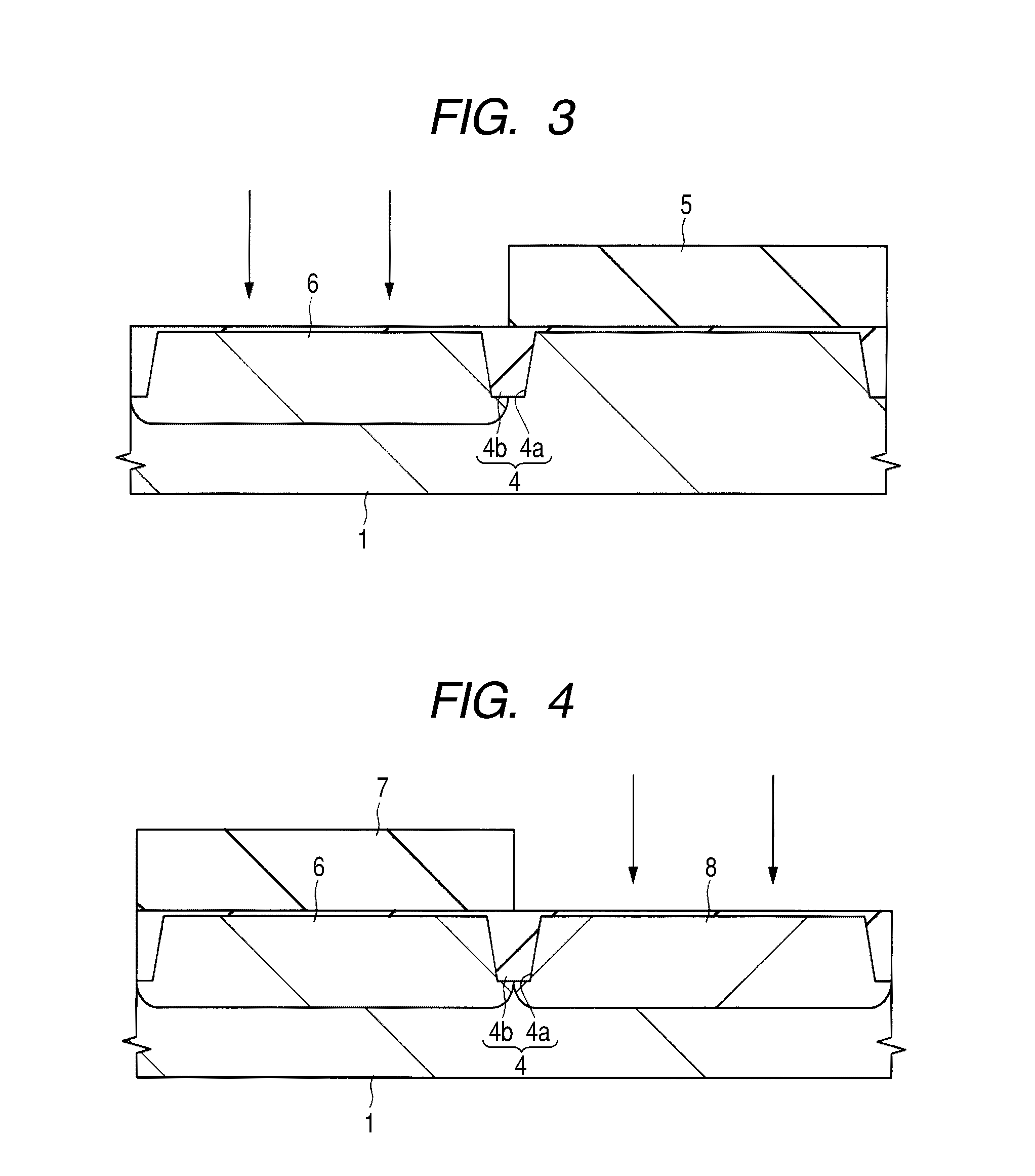
[0071]A method of manufacturing a COMS (Complementary Metal Oxide Semiconductor) device according to a first embodiment of the present invention will be described using FIG. 1 to FIG. 25. FIG. 1 to FIG. 10, FIG. 12, FIG. 17, and FIG. 23 to FIG. 25 are section views of essential parts of a CMOS device, FIG. 11 is a manufacturing process flow diagram of a process to form a silicide layer by the SALICIDE technique, FIG. 13 is a schematic plan view of a device for forming a film of a silicide material, FIG. 14 is a process diagram for forming a film of a silicide material, FIG. 15 is a schematic section view of a dry cleaning processing chamber included in the device for forming a film of a silicide material, FIG. 16 is a schematic section view of a chamber for illustrating a processing process of a semiconductor wafer in the dry cleaning processing chamber included in the device for forming a film of a silicide material, FIG. 18 is a graph diagram for illustrating the temperature rise ...

second embodiment

[0147]A semiconductor device according to a second embodiment resembles that in the first embodiment described above, having a CMOS device in which the platinum-added nickel silicide layer 33 in the PtNiSi phase is formed over the surface of the gate electrode 10n of nMIS and the source / drain diffusion region 16 and over the surface of the gate electrode 10p of pMIS and the source / drain diffusion region 17, but differs from that in the first embodiment described above in the thermal treatment method in the forming process of the platinum-added nickel silicide layer 33. Three divided processes (silicide reaction process, unreacted film removal process, and silicide stabilization process) of the thermal treatment method for forming the platinum-added nickel silicide layer 33 according to the second embodiment will be described below. Conditions of formation of the platinum-added nickel silicide layer 33 in the second embodiment are summarized in Table 3.

TABLE 3Metal filmNiPt(8-14 nm)B...

third embodiment

[0165]A semiconductor device according to a third embodiment, different from that in the first or second embodiment described above, has a CMOS device in which a nickel silicide layer not added with platinum in a NiSi phase is formed over the surface of the gate electrode 10n of nMIS and the source / drain diffusion region 16 and over the surface of the gate electrode 10p of pMIS and the source / drain diffusion region 17. Three divided processes (silicide reaction process, unreacted film removal process, and silicide stabilization process) of a method of forming a nickel silicide layer, in particular, a thermal treatment method of forming a nickel silicide layer according to the third embodiment will be described below. Conditions of formation of the nickel silicide layer in the third embodiment are summarized in Table 4.

TABLE 4Metal filmNi(9 nm)Barrier filmTiN(15 nm)1st RTA400-430° C. 3-10° C. / s2nd RTASpike: 410-635° C.10-250° C. / s

[0166]First, over the main surface of the semiconducto...


PUM


Abstract

To provide a technique capable of improving the reliability of a semiconductor element and its product yield by reducing the variations in the electrical characteristic of a metal silicide layer. After forming a nickel-platinum alloy film over a semiconductor substrate 1, by carrying out a first thermal treatment at a thermal treatment temperature of 210 to 310° C. using a heater heating device, the technique causes the nickel-platinum alloy film and silicon to react with each other to form a platinum-added nickel silicide layer in a (PtNi)2Si phase. Subsequently, after removing the unreacted nickel-platinum alloy film, the technique carries out a second thermal treatment having the thermal treatment temperature higher than that of the first thermal treatment to form the platinum-added nickel silicide layer in a PtNiSi phase. The temperature rise rate of the first thermal treatment is set to 10° C./s or more (for example, 30 to 250° C./s) and the temperature rise rate of the second thermal treatment is set to 10° C./s or more (for example, 10 to 250° C./s).

Description

CROSS-REFERENCE TO RELATED APPLICATION[0001]The present application claims priority from Japanese patent application No. 2008-14408 filed on Jan. 25, 2008, the content of which is hereby incorporated by reference into this application.BACKGROUND OF THE INVENTION[0002]The present invention relates to a manufacturing technique of a semiconductor device and more particularly to a technique which is useful for the application to the manufacture of a semiconductor element having a metal silicide layer.[0003]With the progress of high integration of a semiconductor device, a field effect transistor is miniaturized in accordance with the scaling law, however, there arises a problem that a high-speed operation cannot be obtained even if the field effect transistor is miniaturized because the resistance of a gate, source, and drain increases. Consequently, for example, for a field effect transistor having a gate length of 0.2 μm or less, a SALICIDE (Self Aligned Silicide) technique is under s...

Claims


Application Information

Patent Timeline
IPC IPC(8): H01L21/441
CPCH01L21/28518H01L21/67184H01L21/67207H01L29/7833H01L29/665H01L29/6659H01L21/823835H01L2224/11
Inventor OKADA, SHIGENARIFUTASE, TAKUYAINABA, YUTAKA
Owner RENESAS ELECTRONICS CORP
Why Eureka
Try Eureka