Digital radiographic imaging apparatus

a radiographic and digital technology, applied in the field of digital radiographic imaging, can solve the problems of affecting performance, affecting the performance of conventional imaging arrays, and affecting the charge amplifier of conventional circuit arrangements, so as to reduce the effect of common-mode nois

Active Publication Date: 2009-08-06
CARESTREAM HEALTH INC
View PDF5 Cites 34 Cited by
  • Summary
  • Abstract
  • Description
  • Claims
  • Application Information

AI Technical Summary

Benefits of technology

[0022]The apparatus of the present invention can help to reduce the effects of common-mode noise in the obtained image.

Problems solved by technology

However, the charge amplifiers of the conventional circuit arrangement are subject to common mode noise and other problems that constrain signal quality.
These conventional imaging arrays have limitations which affect performance.
One limitation of digital radiographic arrays employing MIS photosensors, for example, is a reduction in quantum efficiency due to capacitive division of charge between the capacitance of the gate dielectric and capacitance of the semiconductor.
This is a problem with the prior art devices.
In addition to low quantum efficiency, prior art devices also are subject to noise sources, including at least common-mode noise from gate line switching, power supply noise and ripple, and electromagnetic interference (EMI) pickup.
Sources of noise or ripple in the gate line power supplies include noise from switching in switching power supplies, electromagnetic pick-up on power supply bias lines, and circuit noise in the integrated circuit used for generating the row-select clock pulses.
Since this noise is usually temporally uncorrelated with the array readout timing, it cannot be removed by calibration.
A second source of noise in prior-art thin-film transistor arrays for digital radiography is the feed-through of the gate line row-select clock onto the data line.
This coupling is not entirely reversed when the device is subsequently switched off, making it potentially difficult to calibrate for such an offset.
A third source of noise in prior-art thin-film transistor arrays for digital radiography is the electromagnetic pick-up on the data lines.
Whether utilizing MIS photosensors, PIN photodiodes, or other photosensors, these active pixel imaging arrays also suffer from the same difficulties as described above for the passive pixel arrays.
Thus, existing devices exhibit relatively low overall quantum efficiency and are subject to noise sources, including common-mode noise from gate line switching, power supply noise and ripple, and electromagnetic interference (EMI) pickup.
Existing panels do not achieve limited quantum performance, even at radiation levels as high as 1.0 mR.
This coupling is not reversed when the device is subsequently switched on, making it potentially difficult to calibrate for such an offset.
This is not easily compensated by grounding techniques.
The addition of EMI shielding, while it has some beneficial effects, is costly and adds weight.

Method used


Image

  • Digital radiographic imaging apparatus
  • Digital radiographic imaging apparatus
  • Digital radiographic imaging apparatus

Examples


Embodiment Construction

[0044]It is to be understood that elements not specifically shown or described may take various forms well known to those skilled in the art.

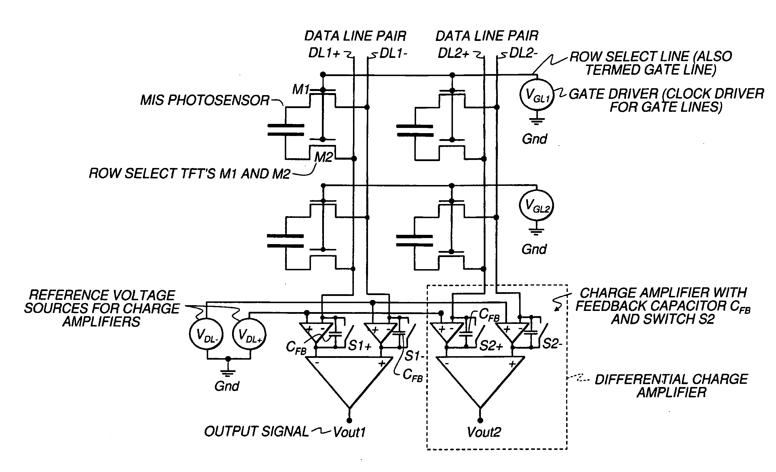
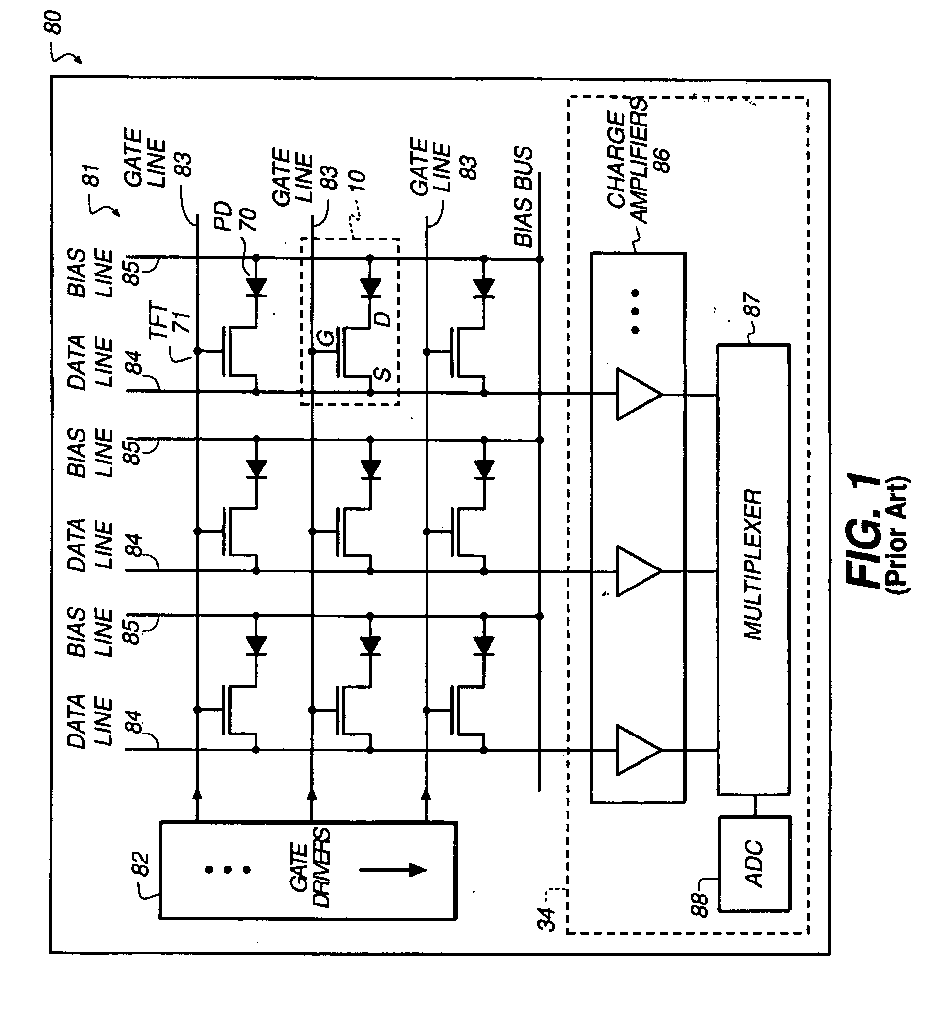
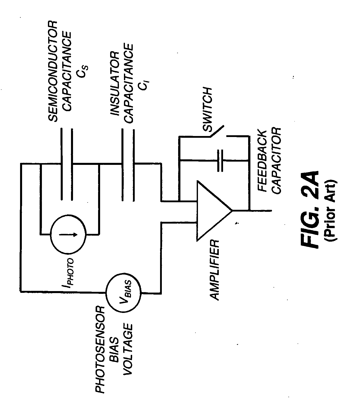
[0045]The schematic diagram of FIG. 3A, illustrated above, showed the conventional charge amplifier arrangement for a 2 column×4 row portion of an array using MIS photosensors and FIG. 3B showed the conventional architecture for a 2 column×4 row portion of an array using PIN photodiodes. In these arrangements, the charge amplifiers typically are located off-panel and connected through a flexible connector or other means. They have a connection to a bias voltage and to the switched signal from a switching element connected to a terminal of photodiode 40 or other photosensor. The second terminal of photodiode 40 can be connected to a bias voltage, with the difference between the first and second bias voltages being the reverse bias set across the photodiode when the gate line is turned on.

[0046]By comparison with Figures A and 3B, FIG. 4A shows a...


PUM


Abstract

A light sensing array has a plurality of electrically isolated photosensors, each photosensor having a first terminal and a second terminal, each of the terminals of each photosensor being isolated from the terminals of the other photosensors, wherein each photosensor responds to an incident light level by producing a charge difference between the first and second terminal. There is a differential circuit selectively coupled to the first and second terminals of one of the photosensors for producing an output signal related to the charge difference between the first and second terminals.

Description

FIELD OF THE INVENTION[0001]This invention generally relates to digital radiographic imaging and more particularly relates to an imaging array using differential readout components.BACKGROUND OF THE INVENTION[0002]A conventional digital radiography (DR) imaging panel acquires image data from a scintillating medium using an array of individual sensors, arranged in a row-by-column matrix, in which each sensor provides a single pixel of image data. Each pixel generally includes a photosensor and a switching element which can be arranged in a planar or a vertical manner, as is generally known in the art. In one known imaging arrangement, a frontplane has an array of photosensitive elements, and a backplane consists of an array of thin-film transistor (TFT) switches. In these imaging devices, hydrogenated amorphous silicon (a-Si:H) is commonly used to form the photodiode and the thin-film transistor switch needed for each pixel, although polycrystalline semiconductors such as laser recry...

Claims


Application Information

Patent Timeline
Patent Type & Authority Applications(United States)
IPC IPC(8): H01L27/146
CPCH04N3/1568H04N5/3577H04N5/357H04N5/32H04N25/617H04N25/60H04N25/00
Inventor TREDWELL, TIMOTHY J.HEILER, GREGORY N.
Owner CARESTREAM HEALTH INC
Why Eureka
Try Eureka