Ruthenium alloy film for copper interconnects

a technology of ruthenium alloy and copper interconnect, which is applied in the direction of chemical vapor deposition coating, semiconductor/solid-state device details, coatings, etc., can solve the problems of limiting the amount of tapered holes, difficult filling of contact holes, and finer and more integrated structures

Active Publication Date: 2009-08-20
ASM JAPAN
View PDF102 Cites 37 Cited by
  • Summary
  • Abstract
  • Description
  • Claims
  • Application Information

AI Technical Summary

Benefits of technology

[0012]To fill connection holes such as contact holes and via holes with Cu, a seed layer having excellent adhesion with Cu film is needed. If a copper plug is used, either with contact holes or via holes, it is also necessary to prevent diffusion of copper. Accordingly, use of a laminate comprising a copper-diffusion barrier layer and a seed layer offering good adhesion with copper as an underlayer is effective in the formation of a copper contact plug. If the deposition speed of Cu film is the same at the bottom and side face of the contact hole, however, it is desired that the contact hole has a shape having a wider opening and tapered toward the bottom. If the contact hole diameter is the same between the opening and bottom, filling such contact hole becomes extremely difficult, and voids called “seams” are formed in the contact plug. The same goes with via plugs. Accordingly, ideally fine contact holes and via holes have a tapered shape if they are to be filled with copper by means of chemical vapor deposition. However, the needs for finer and more integrated structures limit how much the holes can be tapered. Accordingly, new technology to fill these holes without generating seams and voids is needed.
[0021]In the above, the atomic layer deposition (ALD) may be of any type such as thermal or plasma ALD. In the plasma ALD, bias voltage can easily be controlled and applied to the substrate.

Problems solved by technology

If the contact hole diameter is the same between the opening and bottom, filling such contact hole becomes extremely difficult, and voids called “seams” are formed in the contact plug.
However, the needs for finer and more integrated structures limit how much the holes can be tapered.

Method used


Image

  • Ruthenium alloy film for copper interconnects
  • Ruthenium alloy film for copper interconnects
  • Ruthenium alloy film for copper interconnects

Examples


example 1

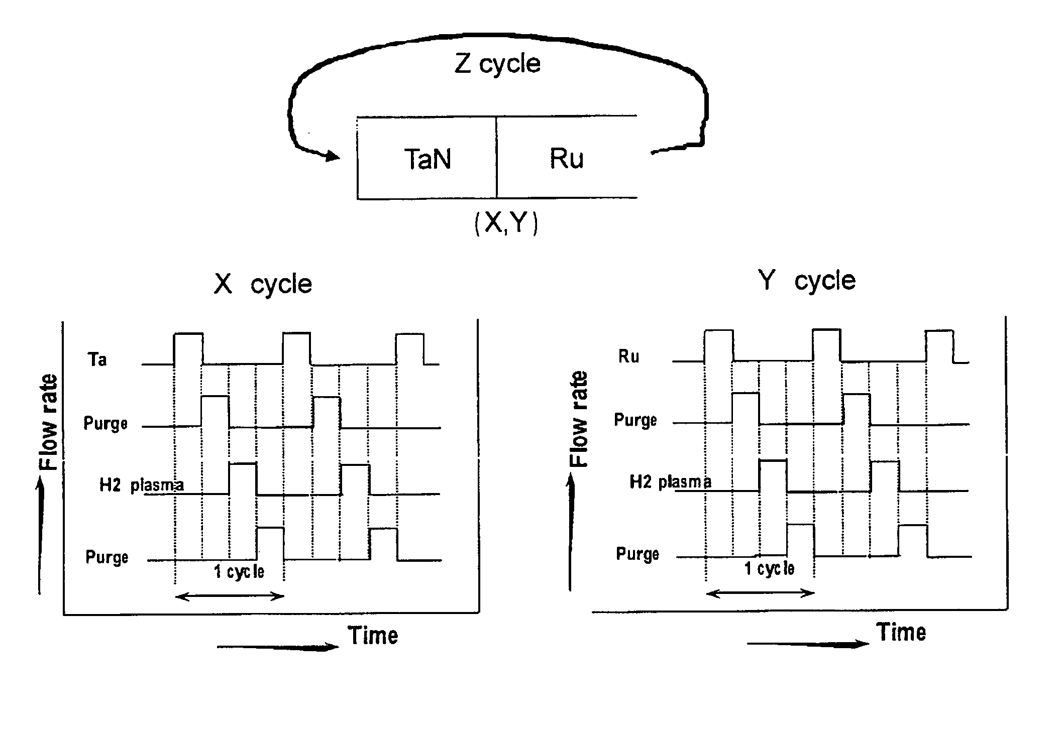
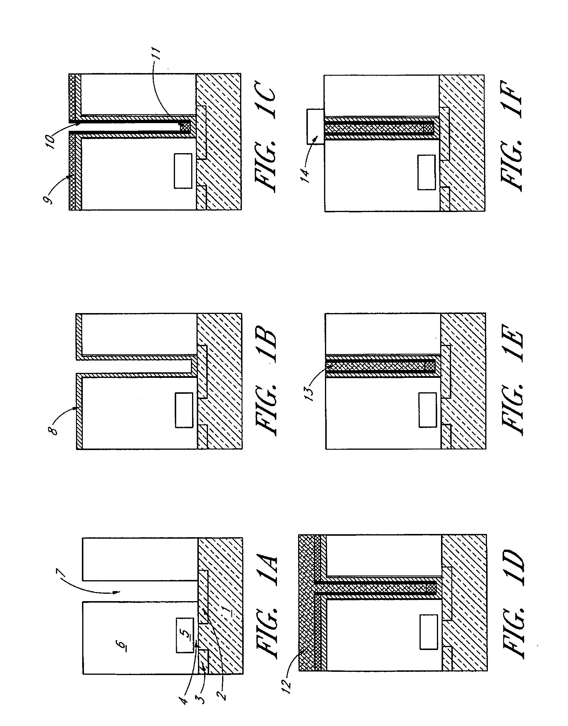
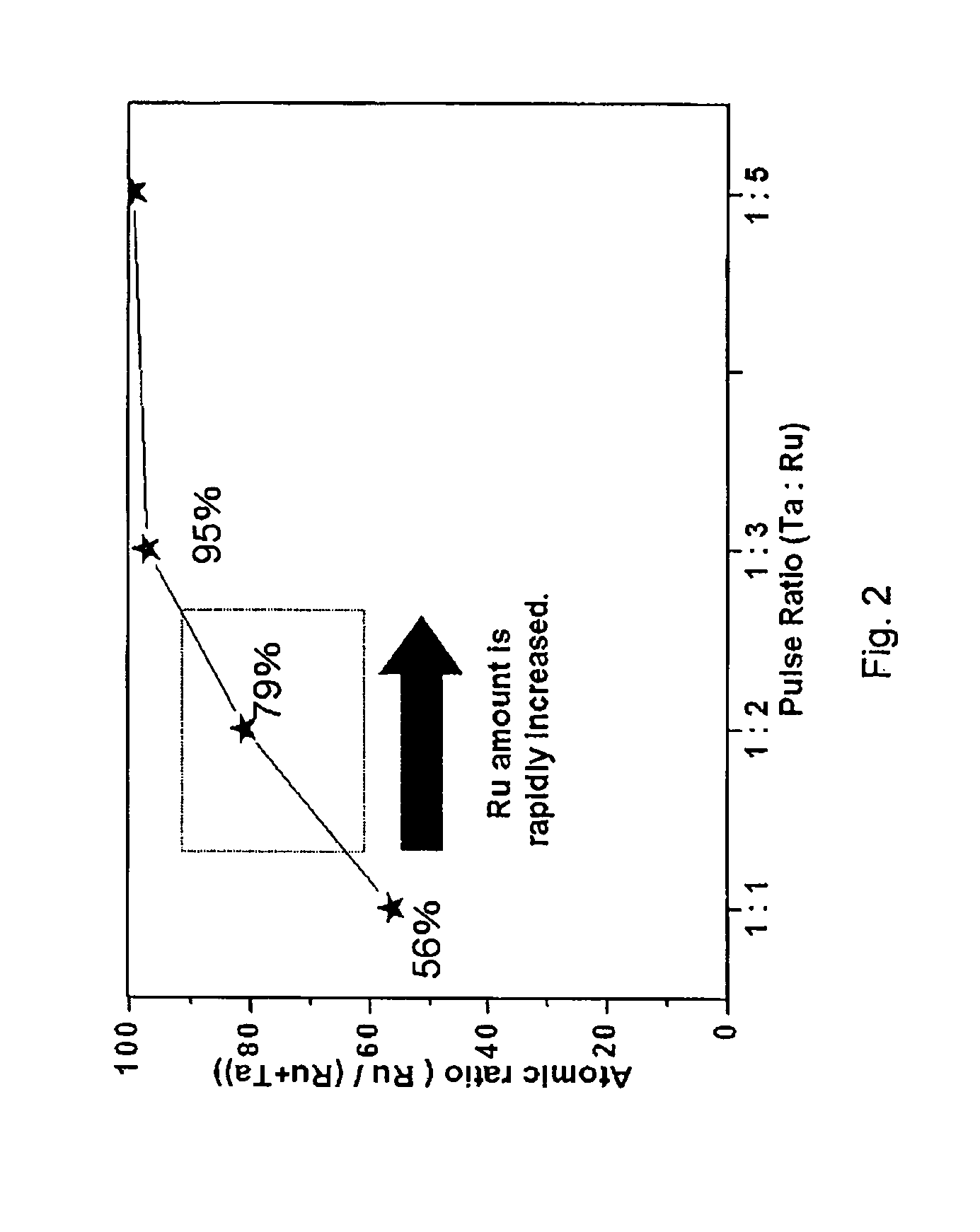
[0189]An example where a Ta—Ru alloy is formed after a TaN film is formed as a Cu barrier over a connection hole similar to the one shown in FIG. 3 using the atomic layer deposition apparatus in FIG. 5 and sequence and process conditions shown in Table 1 below, is explained.

[0190]A substrate in which the connection hole shown in FIG. 3(a) has been formed is introduced into the atomic layer deposition apparatus in FIG. 5. The apparatus shown in FIG. 5 has a cassette loader 201, an atmospheric transfer robot 202, a load lock 203, a vacuum transfer chamber 204, and atomic layer deposition apparatuses 205, 206, 207 shown in FIG. 5. The atomic layer deposition apparatuses 205, 206, 207 are all connected to the same gas line, and also have a Ru material supply part 209, a Ta material supply part 210, a H2 gas supply part 211, and argon gas supply parts 208 for transporting Ru material and Ta material, respectively. The reaction apparatuses 205, 206, 207 are connected to heated gas lines 2...

example 2

[0207]An example of forming a RuTa alloy (RuTaNC film) using the method shown in FIG. 8 through a dual damascene wiring forming process, and then filling the via hole using a Cu film formed by chemical vapor deposition, and filling the wiring layer by Cu formed by electrolytic plating, is explained.

[0208]FIG. 14 is a schematic cross-section view showing the structure of the atomic layer deposition apparatus. Basically, this apparatus has the same structure as what is shown in FIG. 5. A shower head 302 and a substrate heating table 303 are installed in the reaction apparatus 301, and an exhaust 304 for evacuation is connected to the reaction apparatus. An introduction port for mixing material gas 305 is connected to the shower head 302. Connected to this introduction port for mixing material gas 305 is a material gas introduction pipe. Hydrogen gas is introduced through an introduction valve 311 from a flow-rate control 320. Nitrogen gas is connected to the hydrogen gas flow channel ...


PUM

PropertyMeasurementUnit
sizeaaaaaaaaaa
sizeaaaaaaaaaa
thicknessaaaaaaaaaa

Abstract

A method for forming interconnect wiring, includes: (i) covering a surface of a connection hole penetrating through interconnect dielectric layers formed on a substrate for interconnect wiring, with an underlying alloy layer selected from the group consisting of an alloy film containing ruthenium (Ru) and at least one other metal atom (M), a nitride film thereof, a carbide film thereof, and an nitride-carbide film thereof, and (ii) filling copper or a copper compound in the connection hole covered with the underlying layer.

Description

CROSS-REFERENCE TO RELATED APPLICATIONS[0001]This application claims the benefit of U.S. Provisional Application No. 61 / 029,851, filed Feb. 19, 2008, the disclosure of which is herein incorporated by reference in its entirety.BACKGROUND OF THE INVENTION[0002]1. Field of the Invention[0003]The present invention generally relates to formation of copper interconnects or copper wiring filled grooves such as contact holes or via holes, which is suitable for manufacturing fine structure semiconductor devices.[0004]2. Description of the Related Art[0005]In next-generation wiring structures, contact holes that connect diffusion layers and wiring layers on a silicon substrate, and via holes that connect metal wirings, are connection holes for connecting wirings. As semiconductor devices become increasingly finer, aspect ratios of these connection holes are also increasing and concerns are raised over the rise in contact resistance and via resistance. As for contact resistance, tungsten-fille...

Claims


Application Information

Patent Timeline
Patent Type & Authority Applications(United States)
IPC IPC(8): H01L21/44
CPCC23C16/32C23C16/34C23C16/36C23C16/45531H01L21/28562H01L21/76843H01L21/76846H01L2924/0002H01L21/76876H01L21/76877H01L23/53238H01L2924/00
Inventor SHINRIKI, HIROSHIINOUE, HIROAKI
Owner ASM JAPAN
Why Eureka
Try Eureka