Semiconductor processing device and IC card

a processing device and semiconductor technology, applied in the field of semiconductor processing devices, can solve the problems of difficult data transfer from word units to flash memory, increase in chip occupancy area, etc., and achieve the effect of reducing the circuit scale of the second non-volatile memory, reducing the difficulty of deleting stored information, and excellent performan

Inactive Publication Date: 2009-08-27
RENESAS ELECTRONICS CORP
View PDF13 Cites 57 Cited by
  • Summary
  • Abstract
  • Description
  • Claims
  • Application Information

AI Technical Summary

Benefits of technology

[0007]It is another object of the invention to provide a semiconductor processing device capable of enhancing the reliability of information storage for necessary information and implementing a reduction in a size when an on-chip non-volatile memory is utilized for storing data and a program, and furthermore, an IC card.
[0023]For the MOS transistor portion for a selection which has the control gate electrode, comparatively large Gm (a mutual conductance) can easily be obtained at a comparatively low gate voltage because of a relatively low insulating breakdown voltage. Thus, it is possible to relatively increase Gm for a read current from the non-volatile memory cell, thereby contributing to an increase in a reading speed.

Problems solved by technology

For example, it is difficult to transfer data on a word unit to the flash memory in response to the data transfer instruction of the CPU and to rewrite the same data.
The factor of such an increase in the chip occupancy area is hard to disregard in IC card uses in which a chip area is limited at a request of a strength against bending.

Method used


Image

  • Semiconductor processing device and IC card
  • Semiconductor processing device and IC card
  • Semiconductor processing device and IC card

Examples


Embodiment Construction

Microcomputer

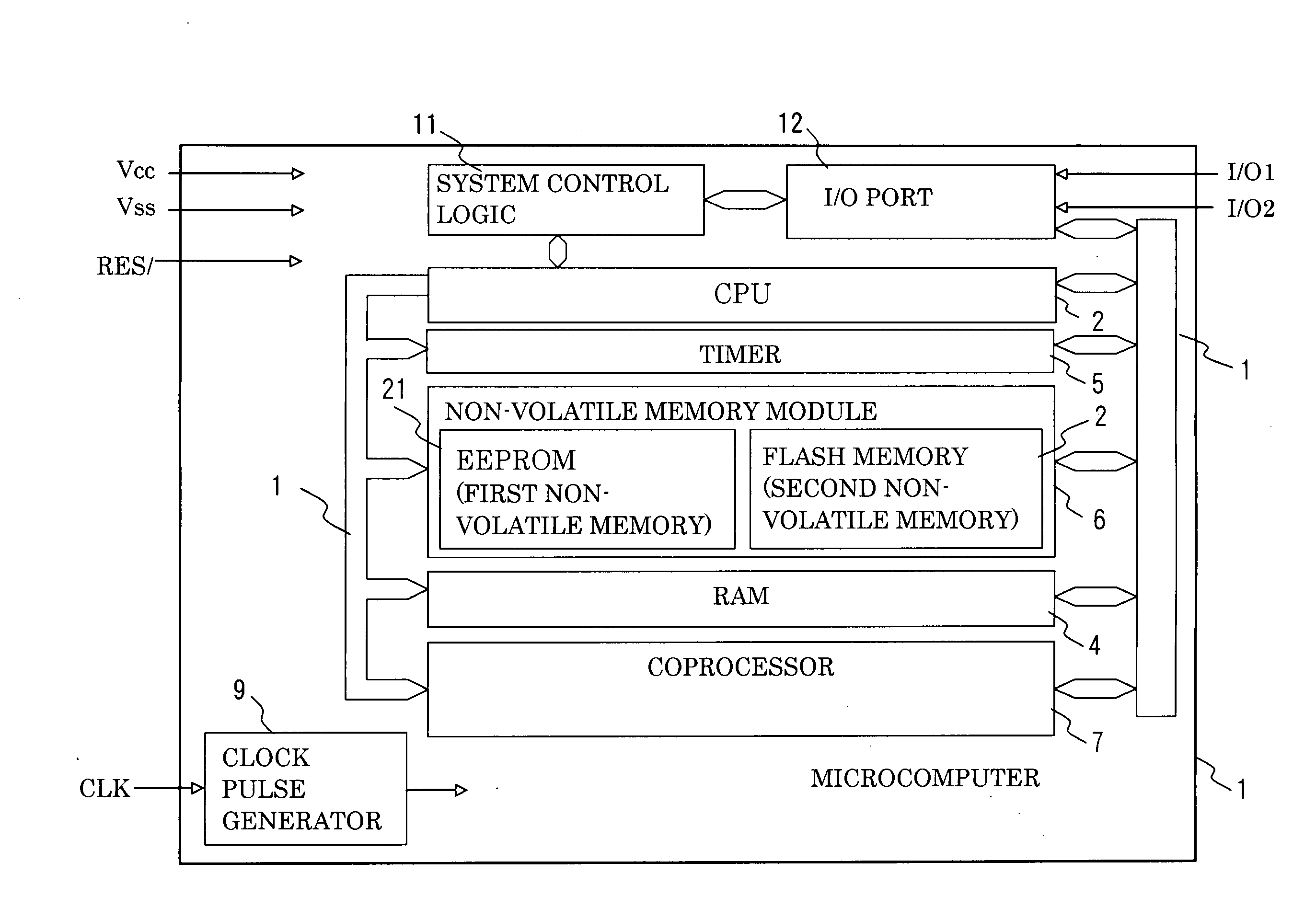
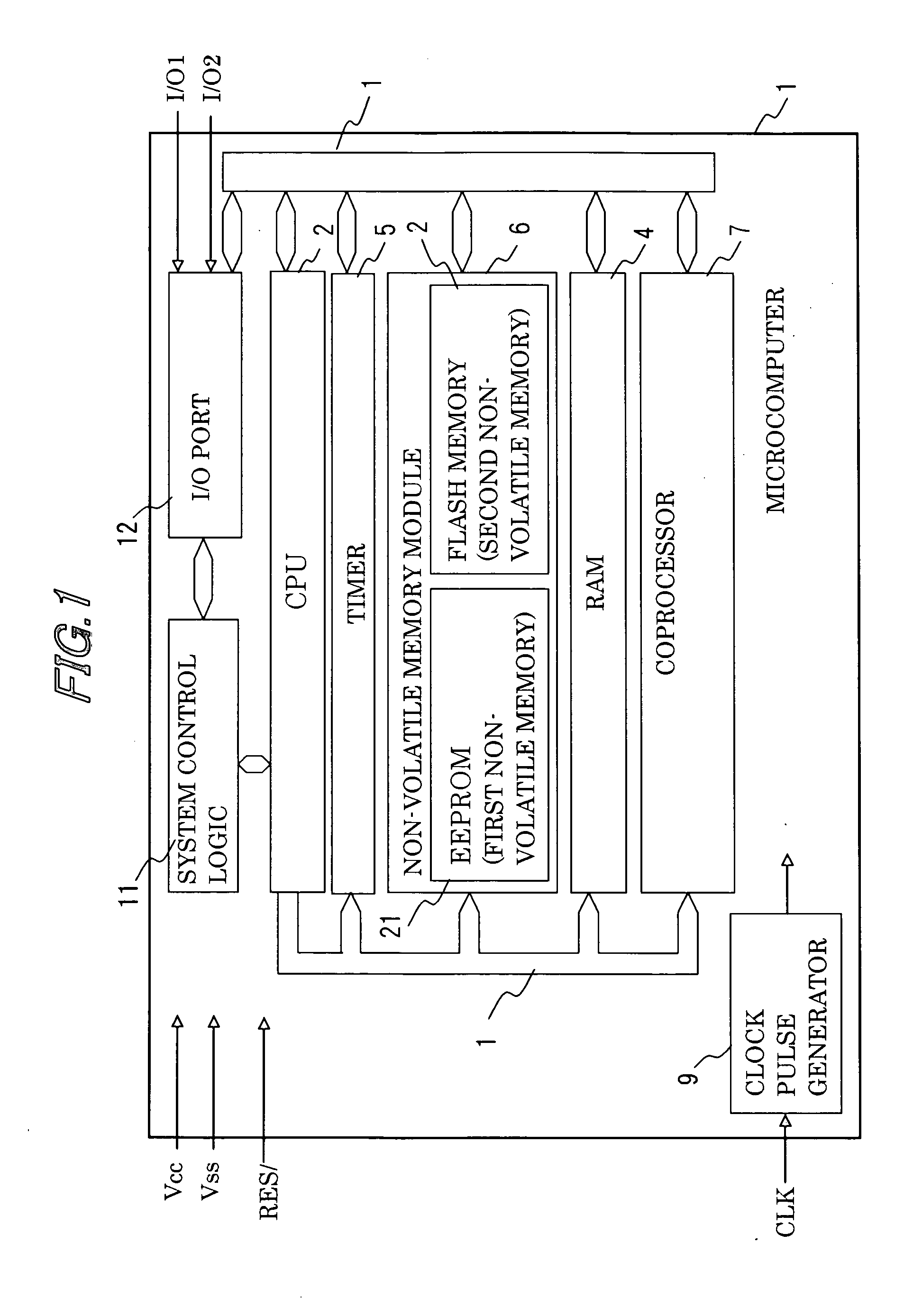
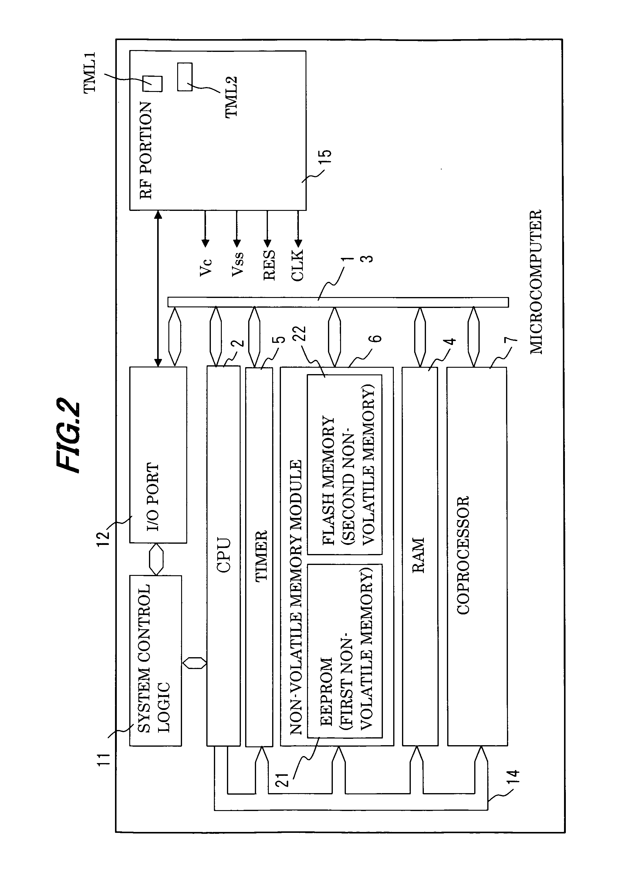
[0075]FIG. 1 illustrates a microcomputer as an example of a semiconductor processing device according to the invention. A microcomputer 1 shown in FIG. 1 is not particularly restricted but is a microcomputer referred to as a so-called IC card microcomputer. The microcomputer 1 shown in FIG. 1 is formed by a technique for manufacturing a semiconductor integrated circuit such as a CMOS on a semiconductor substrate or semiconductor chip, for example, monocrystalline silicon.

[0076]The microcomputer 1 has a CPU 2, an RAM (random access memory) 4, a timer 5, a non-volatile memory module 6, a coprocessor 7, a clock pulse generator 9, a system control logic 11, an input / output port (I / O port) 12, a data bus 13 and an address bus 14.

[0077]The non-volatile memory module 6 is utilized for storing the operation program and data of the CPU 2. The RAM 4 is set to be the work area of the CPU 2 or a temporary storage area for data, and is constituted by an SRAM (Static Random Access Me...


PUM


Abstract

A semiconductor processing device according to the invention includes a first non-volatile memory (21) for erasing stored information on a first data length unit, a second non-volatile memory (22) for erasing stored information on a second data length unit, and a central processing unit (2), and capable of inputting / outputting encrypted data from / to an outside. The first non-volatile memory is used for storing an encryption key to be utilized for encrypting the data. The second non-volatile memory is used for storing a program to be processed by the central processing unit. The non-volatile memories to be utilized for storing the program and for storing the encryption key are separated from each other, and the data lengths of the erase units of information to be stored in the non-volatile memories are defined separately. Therefore, the stored information can efficiently be erased before the execution of a processing of writing the program, and the stored information can be erased corresponding to the data length of a necessary processing unit in the write of the encryption key to be utilized in the calculation processing of the CPU.

Description

FIELD OF THE INVENTION[0001]The present invention relates to a semiconductor processing device such as a microcomputer for an IC card and the IC card, and to an effective technique to be applied to the microcomputer for the IC card which has an electrically rewritable non-volatile memory, for example.BACKGROUND OF THE INVENTION[0002]As an electrically rewritable (A word of rewritable means that it is programmable) non-volatile memory, there has been proposed a so-called flash memory capable of carrying out a write processing and an erase processing on a comparatively large unit such as a batch erase processing on a memory block unit and a page write processing on a word line unit or an EEPROM (Electrically Erasable and Programmable Read Only Memory) capable of carrying out a write processing and an erase processing on a unit of a byte or word to be a calculation processing unit by a CPU. A microcomputer for carrying out on-chip over the EEPROM and a microcomputer for carrying out th...

Claims


Application Information

Patent Timeline
Patent Type & Authority Applications(United States)
IPC IPC(8): G11C11/34G11C16/04G11C5/14G06F12/14G07F7/10G11C16/16
CPCG06Q20/341G06Q20/40975G07F7/084G11C16/16G11C16/0425G11C16/0433G07F7/1008G11C11/005
Inventor TAKAHASHI, MASATOSHIYAMAZOE, TAKANORIKATAYAMA, KOZOTANAKA, TOSHIHIROSHINAGAWA, YUTAKAWATASE, HIROSHIKANAI, TAKEONAGASAKI, NOBUTAKA
Owner RENESAS ELECTRONICS CORP
Why Eureka
Try Eureka