Carbon film

Inactive Publication Date: 2009-09-10
NAT INST OF ADVANCED IND SCI & TECH
View PDF8 Cites 13 Cited by
  • Summary
  • Abstract
  • Description
  • Claims
  • Application Information

AI Technical Summary

Benefits of technology

[0025]A carbon film and a carbon film laminate according to the present invention have optical characteristics of maintaining high transparency even when the grain size becomes small, a high refractive index, and small birefringence; exhibit an excellent electric insulating property; can be coated with satisfactory adhesion, irrespective of the type of the substrate including iron, copper, and plastics; and can be formed at a low temperature.
[0026]As the carbon film and the carbon film laminate according to the invention has the characteristics described above, it can b

Problems solved by technology

However, at present, diamond-like carbon and diamond have the following problems caused by the characteristics of diamond-like carbon and diamond.
However, in a conventional CVD treatment, since the formed MCD has a grain size as large as 0.3 μm to several μm, the obtained MCD film lacks surface flatness and satisfactory transmittance cannot be obtained.
For improving the transmittance, it is necessary to form a flat surface by grinding, and the cost therefor is one of the obstacles to becoming widespread.
As a result, transparency deteriorates, thereby causing quality deterioration of the diamond.
Therefore, this film cannot be utilized in optical application.
Moreover, since electrical resistivity is small, the film cannot be used as an insulator.
However, when MCD is formed by the CVD method which is a typical coating method, it is extremely difficult to synthesize MCD exhibiting no birefringence due to thermal strain and residual stress.
Therefore, it has been a problem that MCD coating is not suitable for optical application.
However, diamond-like carbon film coating and a dia

Method used


Image

  • Carbon film
  • Carbon film
  • Carbon film

Examples


examples

[0118]As follows is a description of examples of the present invention, although the scope of the present invention is by no way limited by these examples.

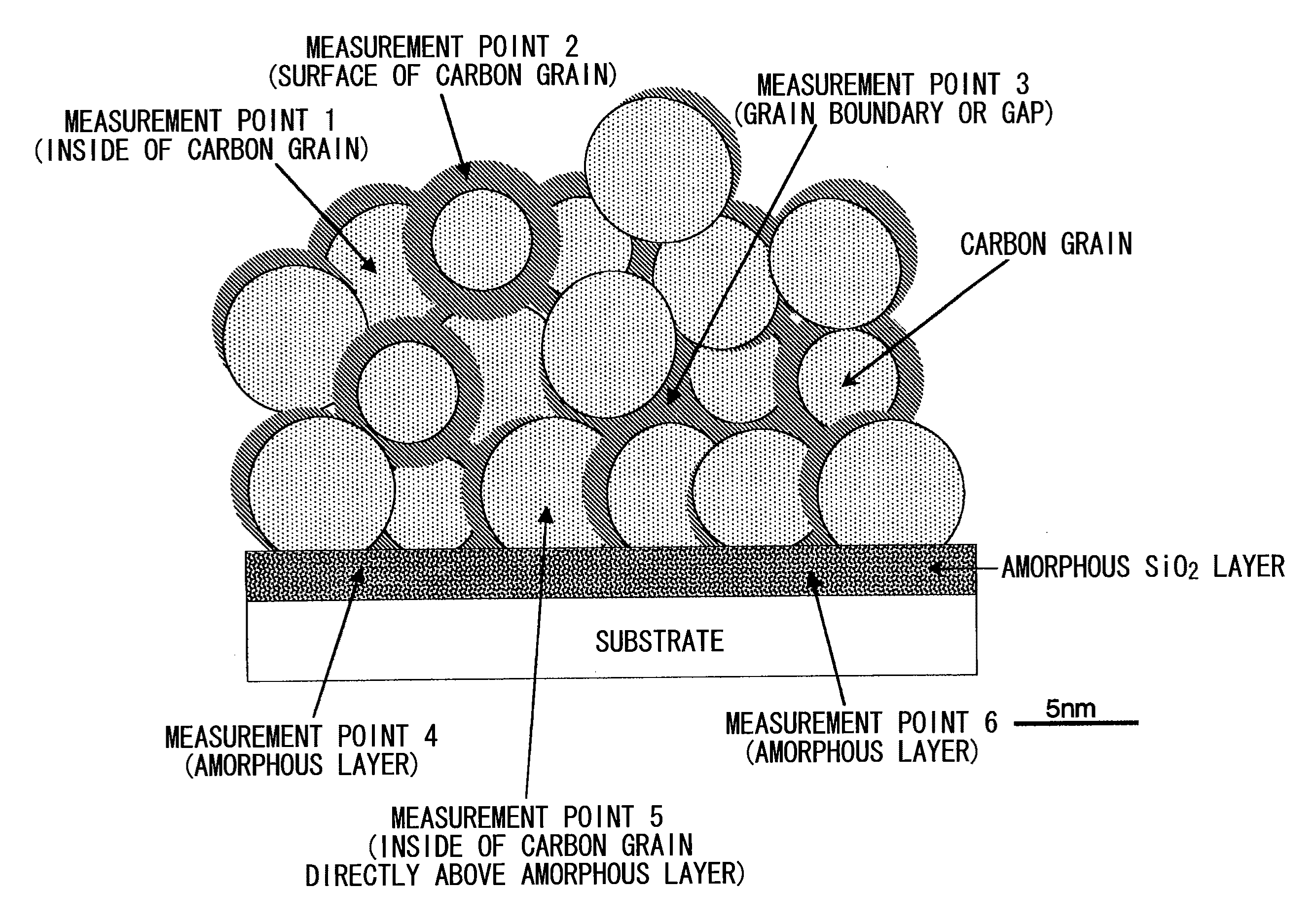
[0119]As a substrate, glass (borosilicate glass and soda lime glass) cut out with a size of 300 mm×300 mm was used. Further, for producing a sample to be evaluated, a wafer-like glass substrate with a 4-inch diameter was also used. For increasing the nucleus formation density of the carbon grains to thereby form a uniform film, the substrate was subjected to a pretreatment (treatment of adhering nano crystal diamond grains) prior to formation of a film.

[0120]In this pretreatment, a colloidal solution (product name: Nanoamand, manufactured by NanoCarbon Research Institute Co., Ltd) in which nano-crystal diamond grains having an average grain size of 5 mm were dispersed in pure water, a solution in which nano-crystal diamond grains of an average grain size of 30 nm or 40 nm (products name: MD30 and MD40 respectively, manufactured by...


PUM

PropertyMeasurementUnit
Grain sizeaaaaaaaaaa

Abstract

A carbon film including: carbon grains having substantially the same grain size in the range of 1 nm to 1,000 nm, and preferably in the range of 2 nm to 200 nm, in the thickness-wise direction of the carbon film; and an amorphous substance for suppressing generation of impurities accompanied by formation of the carbon grains and/or for suppressing growth of said carbon grains, the amorphous substance existing at least on the surfaces of the carbon grains in a grain boundary between the carbon grains and/or gaps between the carbon grains. Such a carbon film has excellent optical properties such as high transparency, a high refractive index and small birefringence, and exhibits excellent electrical insulation. Further, the carbon film can be coated on various substrates with high adhesion and can be formed at a low temperature. Therefore, the carbon film is extremely useful for application to an optical device, a wrist watch, an electronic circuit substrate, a grinding tool or a protection film.

Description

TECHNICAL FIELD[0001]The present invention relates to a carbon film and a carbon film laminate having new properties; an optical device, an optical glass, a lens, a wrist watch, an electronic circuit substrate, a grinding tool, a low-friction protection film, a vehicle engine component, a mechanical component, and a health appliance provided with the same; and a method and apparatus for manufacturing the carbon film and the carbon film laminate.BACKGROUND ART[0002]A carbon-based thin film has various excellent characteristics such as high hardness, thermal conductivity, an electric insulating property, transparency, a high refractive index, chemical resistance, a low friction property, and a low abrasion property. Recently, due to its excellent environmental compatibility and biocompatibility, it has been desired to use a carbon-based thin film as a coating for improving the performance of various substrates. Especially, a diamond-like carbon film and a diamond film are thin carbon-...

Claims


Application Information

Patent Timeline
IPC IPC(8): B32B27/04C23C16/26
CPCC03C17/007C03C17/3411C03C2217/42C03C2218/153C23C16/0272C23C16/26Y10T428/269C23C16/277C23C16/279C23C16/511G04B39/006Y10T428/268C23C16/27
Inventor HASEGAWA, MASATAKATSUGAWA, KAZUOKOGA, YOSHINORIISHIHARA, MASATOUIIJIMA, SUMIO
Owner NAT INST OF ADVANCED IND SCI & TECH
Why Eureka
Try Eureka