Eureka AIR delivers breakthrough ideas for toughest innovation challenges, trusted by R&D personnel around the world.

Integrated passive device and method with low cost substrate

a passive device and low-cost technology, applied in the direction of semiconductor devices, electrical apparatus, semiconductor/solid-state device details, etc., can solve the problems of low a resistivity to be used, the inability to fit all of the desired components into the finished wireless device, and the inability to meet the requirements of the final wireless device, so as to increase the effective resistivity of the silicon substrate and high resistivity.

Inactive Publication Date: 2009-09-24
FREESCALE SEMICON INC
View PDF13 Cites 11 Cited by
  • Summary
  • Abstract
  • Description
  • Claims
  • Application Information

AI Technical Summary

Benefits of technology

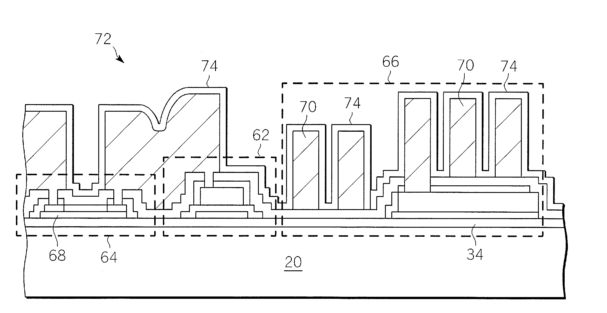
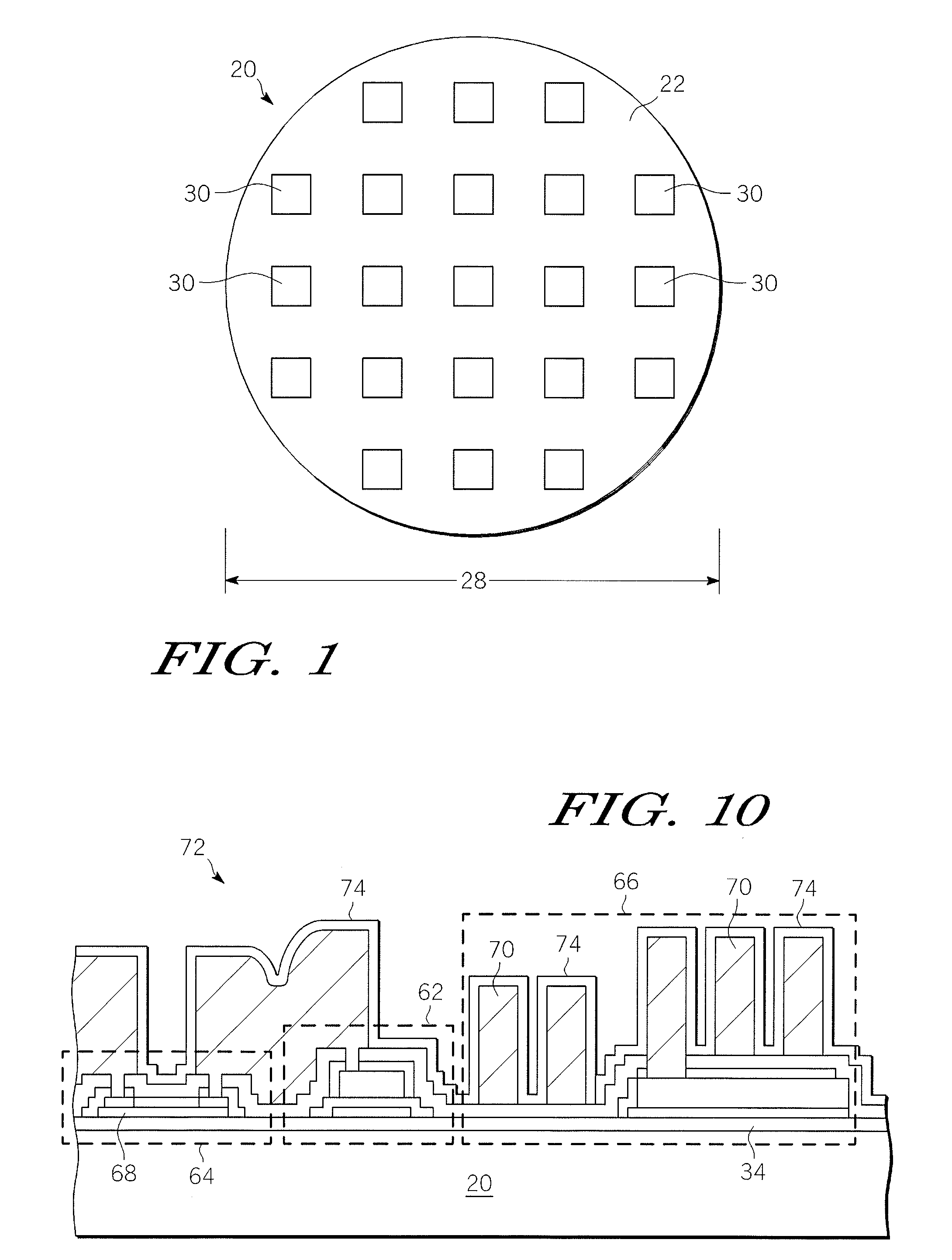
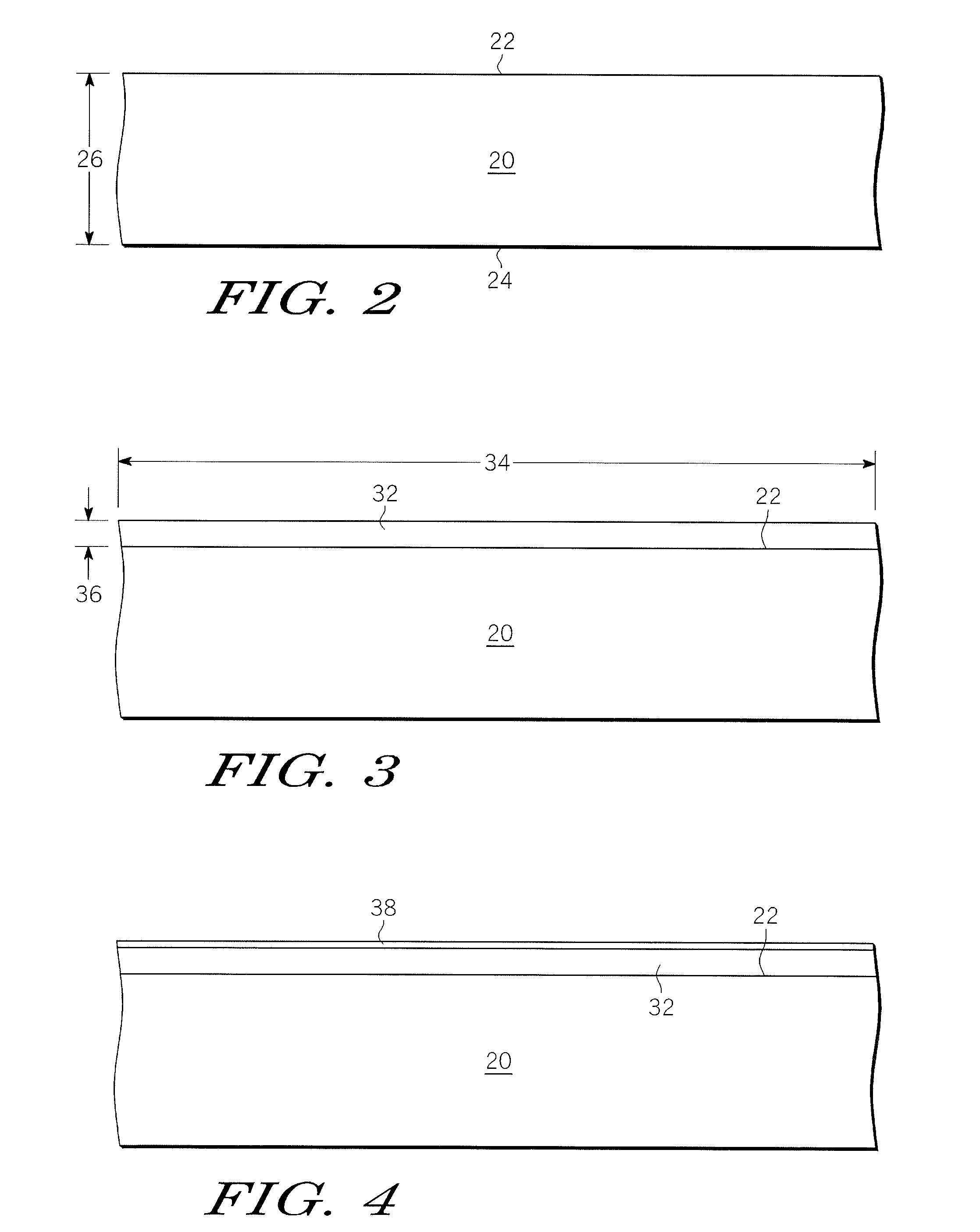
[0024]FIG. 1 to FIG. 10 illustrate a method for forming an integrated passive device (IPD). An initial dielectric layer is formed on a silicon substrate, preferably a high resistivity (HR) silicon substrate, and at least one passive electronic component is formed over the initial dielectric layer. A combination of the choice of material for the initial dielectric layer, deposition process for the initial dielectric layer and pre-treatment of the silicon surface prior to deposition of the initial dielectric layer, can increase the effective resistivity of the silicon substrate so that the silicon substrate is suitable for use in IPDs used in, for example, wireless communications devices, as well as other radio frequency (RF) devices, and is comparable in performance to much more expensive substrate materials such as, for example, GaAs.

Problems solved by technology

However, as performance demands continue to increase while the overall size of the finished devices decreases, it is becoming increasingly difficult to fit all of the desired components into the finished wireless device.
However, in order to optimize performance, IPDs are typically formed on relatively high resistivity substrates, such as those made of gallium arsenide (GaAs), glass, quartz, or sapphire, as opposed to silicon, which is generally considered to have too low a resistivity to be used in IPDs for wireless communication devices.
One problem associated with forming IPDs on such high resistivity substrates is that these materials are considerably more expensive than silicon.
These process modifications further increase manufacturing costs, as well as production time.

Method used


Image

  • Integrated passive device and method with low cost substrate
  • Integrated passive device and method with low cost substrate
  • Integrated passive device and method with low cost substrate

Examples


first embodiment

[0058] there is provided a method of forming an integrated passive device (IPD) comprising, forming an insulating initial dielectric layer comprising aluminum nitride over a silicon substrate, and forming at least one passive electronic component over the insulating initial dielectric layer. According to a further embodiment, the insulating initial dielectric layer is an aluminum nitride layer and the at least one passive electronic component comprises at least one of a capacitor, a resistor, an inductor and a transmission line. According to a still further embodiment, the insulating initial dielectric layer comprises an aluminum nitride layer and another dielectric layer. According to a yet further embodiment, the another dielectric layer comprises silicon nitride. According to a still yet further embodiment, the another dielectric layer comprises silicon oxide. According to a yet still further embodiment, the insulating initial dielectric layer is formed at a temperature that is b...

second embodiment

[0059] there is provided a method for forming an integrated passive device (IPD) comprising, providing a silicon substrate with a resistivity equal to or greater than about 1000 ohm-cm and having an outer surface, exposing the outer surface of the substrate to a surface damage causing circumstance, forming an initial dielectric layer comprising aluminum nitride, silicon nitride, TEOS or a combination thereof over the outer surface, and forming a plurality of passive electronic components over the initial dielectric layer. According to a further embodiment, the surface damage causing circumstance is exposure to a plasma formed using a substantially inert gas. According to a still further embodiment, the substantially inert gas is argon. According to a yet further embodiment, the surface damage causing circumstance is deposition of a sputtered aluminum nitride layer. According to a still yet further embodiment, the plurality of passive electronic components comprises at least one of a...

third embodiment

[0060] there is provided a microelectronic assembly comprising, a silicon substrate with a resistivity of at least 1000 ohm-cm, an initial dielectric layer comprising aluminum nitride, and a plurality of passive electronic components formed over the initial dielectric layer. According to a further embodiment, the initial dielectric layer further comprises silicon nitride. According to a still further embodiment, the plurality of passive electronic components comprises at least one of a capacitor, a resistor, a transmission line and an inductor. According to a yet further embodiment, the plurality of passive electronic components jointly form a harmonic filter, coupler, or a transformer. According to a still yet further embodiment, the microelectronic assembly further comprises an integrated circuit coupled to the plurality of passive electronic components.


PUM


Abstract

According to one aspect of the present invention, a method of forming a microelectronic assembly, such as an integrated passive device (72), is provided. An insulating initial dielectric layer (32) comprising charge trapping films of, for example, aluminum nitride or silicon nitride or silicon oxide or a combination thereof, is formed over a silicon substrate (20). At least one passive electronic component (62) is formed over the initial dielectric layer (32). In an embodiment where silicon nitride or oxide is used in the initial dielectric layer (32) in contact with the silicon substrate (20), it is desirable to pre-treat the silicon surface (22) by exposing it to a surface damage causing treatment (e.g. an argon plasma) prior to depositing the initial dielectric layer, to assist in providing carrier depletion near the silicon surface around zero bias. RF loss in integrated passive devices using such silicon substrates is equal or lower than that obtained with GaAs substrates.

Description

FIELD OF THE INVENTION[0001]The present invention generally relates to microelectronic assemblies and a method for forming microelectronic assemblies, and more particularly relates to integrated passive devices (IPDs) with low cost substrates and a method for forming such IPDs.BACKGROUND OF THE INVENTION[0002]In recent years, wireless communication devices, such as cellular phones, have continued to offer an ever increasing amount of features to users, along with improved performance and computing power, while the overall size of the devices has continued to decrease. One important type of components found in such devices is referred to as “passive electronic components,” including capacitors, resistors, transmission lines and inductors. Often, these components work together to perform various electronic functions such as harmonic filtering, decoupling, impedance matching, and switching.[0003]In years past, discrete passive electronic components were used in wireless communication d...

Claims


Application Information

Patent Timeline
IPC IPC(8): H01L29/00H01L21/20
CPCH01L23/5227H01L23/5228H01L27/016H01L2924/3011H01L2924/0002H01L2924/00
Inventor DALY, TERRY K.COSTELLO, KERI L.COTRONAKIS, JAMES G.FENDER, JASON R.HUGHES, JEFF S.MITRA, AGNIREYES, ADOLFO C.
Owner FREESCALE SEMICON INC
Why Eureka
Eureka Blog
Learn More