Large-area pin diode with reduced capacitance

a pin diode and capacitance reduction technology, applied in the field of high-energy radiation detectors, can solve the problems of large capacitance that is difficult to handle by a readout circuitry, inefficient external detectors, and inefficiency of collection, so as to improve the signal to noise ratio, reduce the capacitance of the pixel's pin diode, and improve the effect of fom

Active Publication Date: 2009-10-01
THE RES FOUND OF STATE UNIV OF NEW YORK
View PDF5 Cites 6 Cited by
  • Summary
  • Abstract
  • Description
  • Claims
  • Application Information

AI Technical Summary

Benefits of technology

[0013]A reasonable figure of merit (FoM) for the pixel performance is the ratio of expected number of photons incident of the pixel's PIN diode in response to the typical Compton interaction that occurred within the volume of said pixel, to the capacitance of the pixel's diode. In the prior art design, at least for small enough pixels, both parameters in the FoM scale with the diode area and hence their ratio

Problems solved by technology

External detectors are inefficient for the following reason.
The escape cone accommodates only about 2% of isotropic scintillation, signifying the inefficiency of collection.
In principle one can use a single photodiode over the entire area of the chip, but for a chip of large area this may introduce a large capacitance that is difficult to han

Method used


Image

  • Large-area pin diode with reduced capacitance
  • Large-area pin diode with reduced capacitance
  • Large-area pin diode with reduced capacitance

Examples


Embodiment Construction

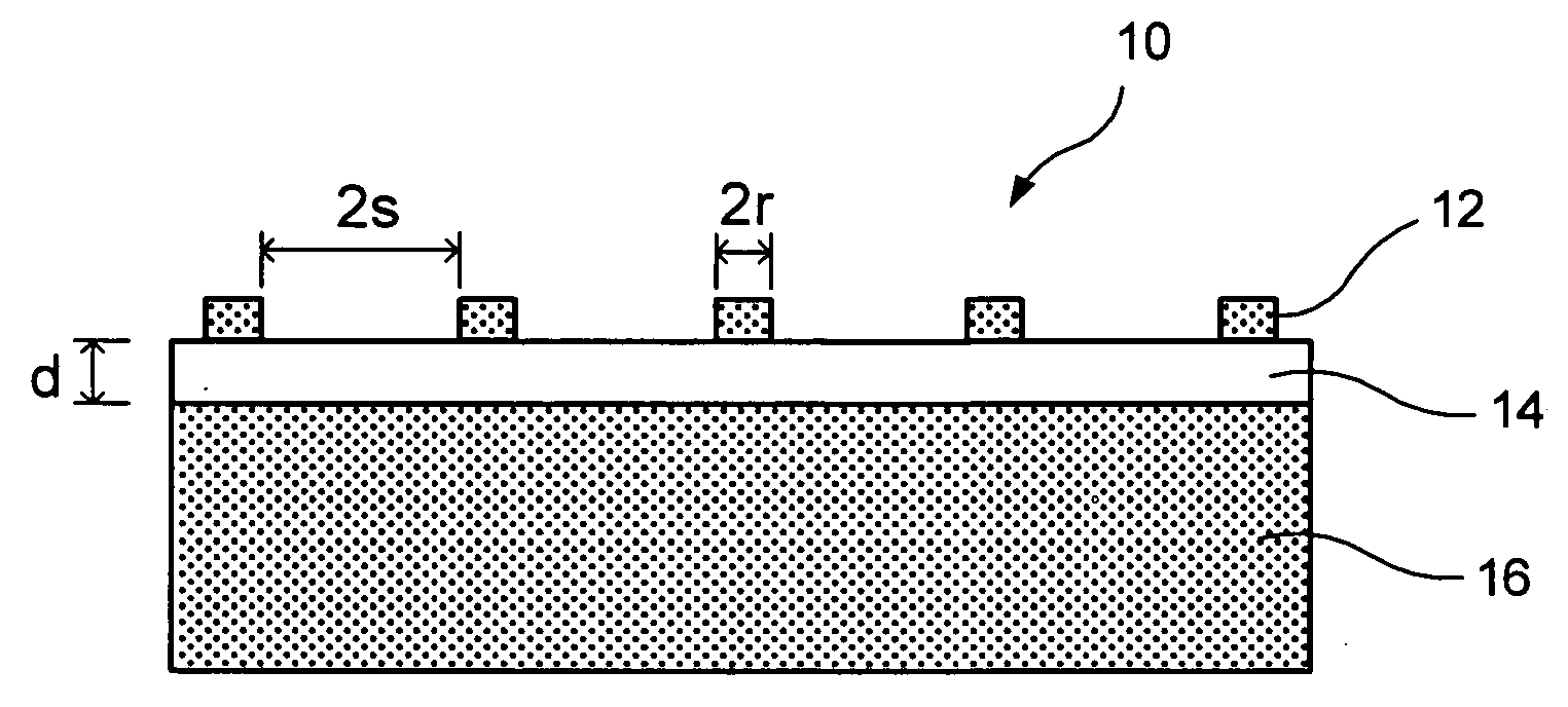
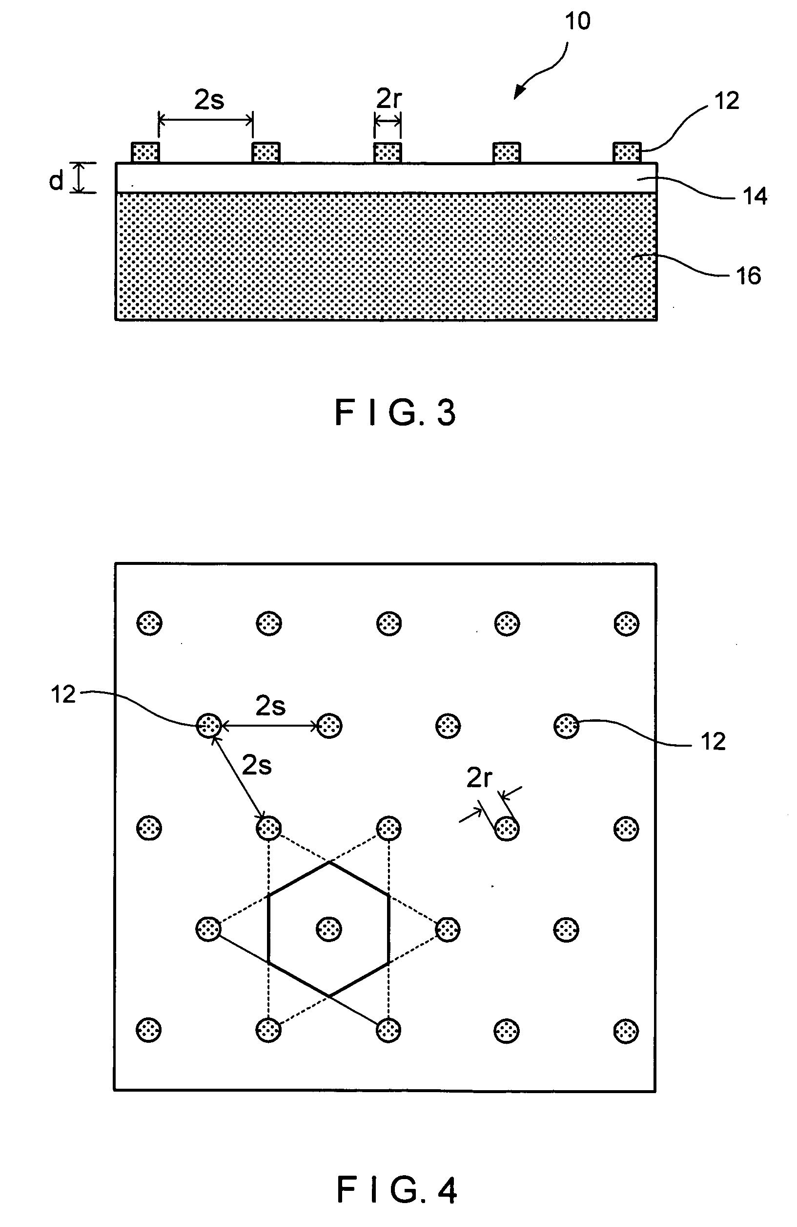
[0033]Referring now to FIGS. 3 and 4, illustrating essential features of one aspect of the invention and showing a large PIN diode 10 with small capacitance. The cross-section of the PIN diode is depicted in FIG. 3, where collector contacts 12 (p-type, for example) are shown disposed on the intrinsic (depleted) region 14 disposed on the n region 16. The surface between the contacts is passivated by dielectric, such as for example, a silicon nitride layer. FIG. 4 illustrates the top view of the contacts.

[0034]The total area of the collector contacts 12 is much smaller than the area of the diode and the contacts are spaced from each other by the distance 2s. Such distance should be not too large so that the travel time of holes over the distance s is much smaller than the lifetime of holes in the intrinsic region. All contacts 12 are connected together by thin metallic lines (not shown in FIGS. 3 and 4), which are disposed over a dielectric layer covering all contacts 12 and accessing...


PUM


Abstract

The invention provides a design of PIN diode having a low capacitance and a large area of effective collection of photo-generated charge. The low capacitance is obtained by replacing a continuous collector layer in the diode by a sparse array of collector disks interconnected by narrow metallic runners at a different structural level separated from the collector discs by an interlevel dielectric.

Description

[0001]THIS NON-PROVISIONAL APPLICATION CLAIMS PRIORITY UNDER 35 USC 119 (e) OF U.S. PROVISIONAL APPLICATION SER. NO. 61 / 072,229 FILED BY DR. SERGE LURYI ON MAR. 28, 2008.FIELD OF THE INVENTION[0002]The present invention relates in general to high-energy radiation detectors, and in particular it relates to radiation detectors based on direct-gap semiconductor scintillator wafers, endowed with an epitaxial photodiode on a surface thereof.BACKGROUND OF THE INVENTION[0003]Referring now to FIGS. 1 and 2 illustrating the prior-art two dimensional (2D) pixel architectures. FIG. 1, shows the cleaved pixel design with device area being about 1 mm×1 mm. The key motivation for this design is as follows. Spatial independence of the scintillation flux on the pixel photodiodes should be ensured, so that the readout would be the same irrespective of where the interaction occurs in the volume of pixel. Due to the high refractive index of InP, only a small fraction of radiation impinging on the side...

Claims


Application Information

Patent Timeline
IPC IPC(8): H01L31/0216H01L21/20
CPCH01L27/14663H01L31/085H01L31/02322H01L31/022408Y02E10/548
Inventor LURYI, SERGE
Owner THE RES FOUND OF STATE UNIV OF NEW YORK
Why Eureka
Try Eureka