

Light emitting device
a light-emitting device and light-emitting technology, applied in the direction of semiconductor devices, electrical devices, transistors, etc., can solve the problem of inability to increase the internal quantum efficiency, and achieve the effect of improving the internal quantum efficiency and light extraction efficiency
- Summary
- Abstract
- Description
- Claims
- Application Information
AI Technical Summary
Benefits of technology
Problems solved by technology
Method used
Image

Examples
first embodiment
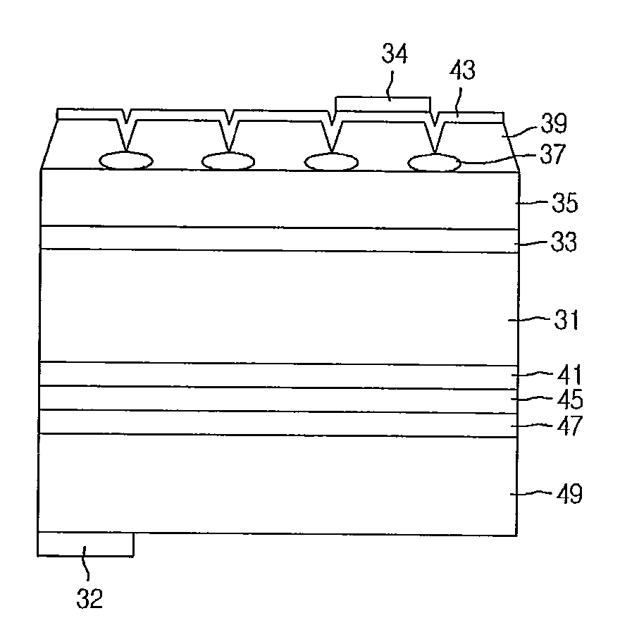
[0014]FIG. 1 is a sectional view showing a light emitting device according to a first embodiment.
[0015]As shown in FIG. 1, the light emitting device according to the first embodiment can include a first conductive semiconductor layer 11, a light emitting layer 13, a protective layer 15, a nano-layer 17, and a second conductive semiconductor layer 19. The light emitting layer 13 can be formed on the first conductive semiconductor layer 11. The protective layer 15 can be formed on the light emitting layer 13. The nano-layer 17 can be formed on the protective layer 15. The second conductive semiconductor layer 19 can be formed on the nano-layer 17.
[0016]The first conductive semiconductor layer 11 can include an electron injection layer, and the second conductive semiconductor layer 19 can include a hole injection layer. In addition, the first conductive semiconductor layer 11 can include the hole injection layer, and the second conductive semiconductor layer 19 can include the electron...
second embodiment
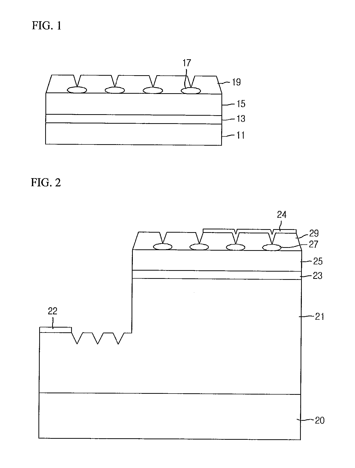
[0025]FIG. 2 is a sectional view showing a light emitting device according to the second embodiment. Particularly, FIG. 2 is a sectional view showing a horizontal light emitting device according to the second embodiment, but the embodiment is not limited thereto. Hereinafter, the structure of the light emitting device and a method for manufacturing the light emitting device according to the second embodiment will be described with reference to FIG. 2.
[0026]A first conductive semiconductor layer 21 can be formed on a substrate 20. The first conductive semiconductor layer 21 can include an electron injection layer. The electron injection layer can include a high-quality thin film layer based on AlxInyGa1-x-yN (0≦x, y≦1) and having electrical conductivity. When the substrate 20 is a hetero substrate, the substrate 20 can include silicon (Si), sapphire, silicon carbide (SiC), zinc oxide (ZnO), or other metal oxide materials. When the substrate 20 is a homo substrate, the substrate 20 ca...
third embodiment
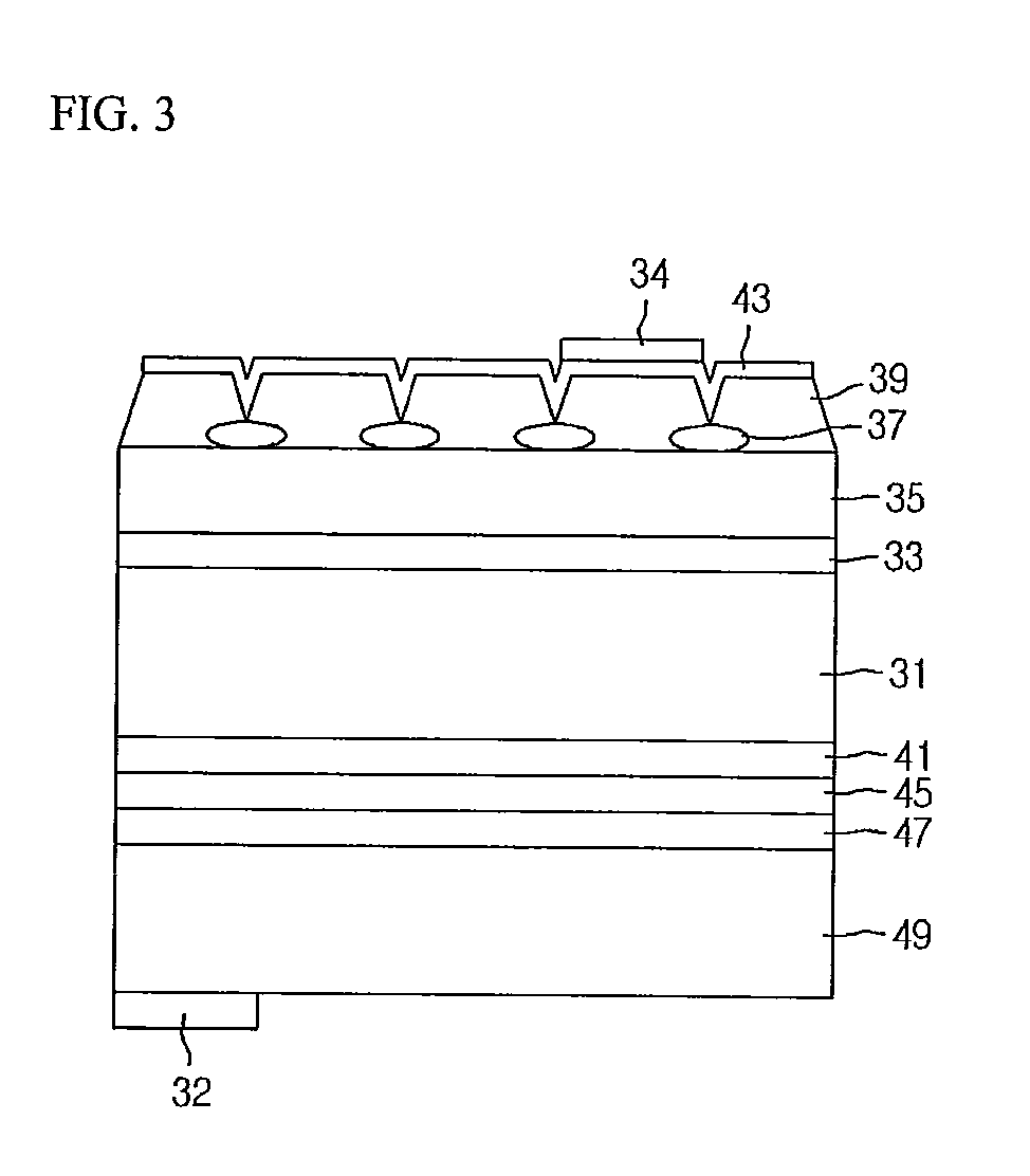
[0061]FIG. 3 is a sectional view showing a light emitting device according to a third embodiment. Particularly, FIG. 3 is a sectional view showing a vertical light emitting device, and the third embodiment is not limited thereto.
[0062]Hereinafter, a method for manufacturing the light emitting device according to the third embodiment will be described with reference to FIG. 3. A first conductive semiconductor layer 31 according to the third embodiment can include an N-type semiconductor layer, but the embodiment is not limited thereto.
[0063]A metal organic chemical vapor deposition (MOCVD) system can be used to grow a thin film of a nitride semiconductor, but the third embodiment is not limited thereto. A substrate can include sapphire, but the embodiment is not limited thereto. Ammonia can be used as a nitrogen source, and hydrogen (H) and oxygen (O) can be used as carrier gas. Gallium (Ga), indium (In), and aluminum (Al) can be used as a metal organic source. Silicon (Si) can be us...
PUM
 Abstract
Description
Claims
Application Information