Metallized conductive strap spacer for soi deep trench capacitor

a technology of conductive straps and capacitors, applied in the direction of semiconductor devices, electrical equipment, transistors, etc., can solve the problems of reducing the thickness of the top semiconductor layer, affecting the operation of the semiconductor, and presenting a difficulty in the formation of buried straps employed

Active Publication Date: 2009-10-15
IBM CORP
View PDF6 Cites 39 Cited by
  • Summary
  • Abstract
  • Description
  • Claims
  • Application Information

AI Technical Summary

Benefits of technology

[0022]forming a field effect transistor comprising a source region, wherein the source region laterally abuts the node dielectric;

Problems solved by technology

Despite such enhanced performance, however, such UTSOI substrates presents a difficulty in the formation of a buried strap employed to electrically connect the deep trench capacitor to an access transistor, which is required in an embedded DRAM cell or other devices in which electrical connection to the deep trench capacitor is controlled by an access transistor.
Specifically, difficulty in recess control of a conductive fill material arises as the thickness of a top semiconductor layer is reduced below the 100 nm range.
In this case, the leakage current between a passing word line over the shallow trench isolation structure and the buried strap increases to degrade the performance of the device incorporating the deep trench capacitor or even render the device non-functional.

Method used


Image

  • Metallized conductive strap spacer for soi deep trench capacitor
  • Metallized conductive strap spacer for soi deep trench capacitor
  • Metallized conductive strap spacer for soi deep trench capacitor

Examples


first embodiment

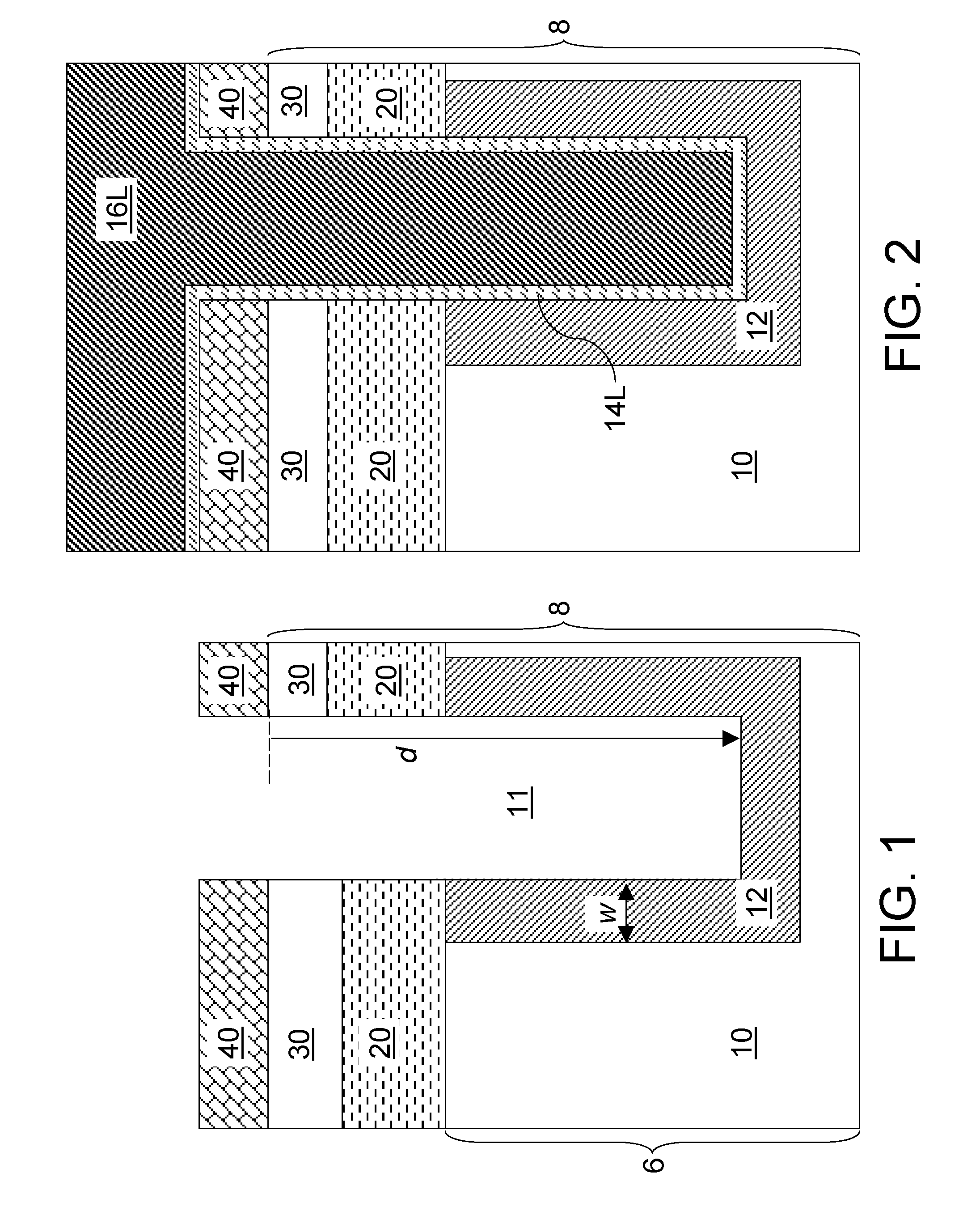
[0056]Referring to FIG. 1, a first exemplary semiconductor structure according to the present invention comprises a semiconductor-in-insulator (SOI) substrate 8 containing a top semiconductor layer 30, a buried insulator layer 20, and a bottom semiconductor layer 6. Each of the top semiconductor layer 30 and the bottom semiconductor layer 6 comprises a semiconductor material. The semiconductor material of the top semiconductor layer 30 and the semiconductor material of the bottom semiconductor layer 6 may be the same, or different. The semiconductor materials for the top semiconductor layer 30 and the bottom semiconductor layer 6 may be selected from, but is not limited to, silicon, germanium, silicon-germanium alloy, silicon carbon alloy, silicon-germanium-carbon alloy, gallium arsenide, indium arsenide, indium phosphide, III-V compound semiconductor materials, II-VI compound semiconductor materials, organic semiconductor materials, and other compound semiconductor materials. Typic...

fourth embodiment

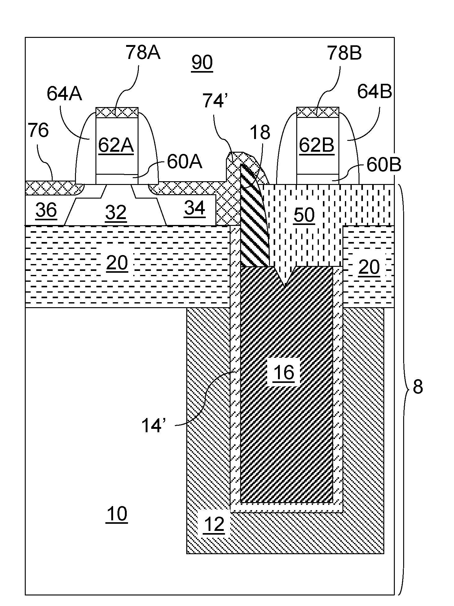
[0097]Referring to FIG. 20, a fourth exemplary semiconductor structure according to the present invention is derived from the third exemplary semiconductor structure of FIG. 18. The divot 19 is subjected to an isotropic etch that removes the sidewall of the source region 34 by a lateral etch, thereby forming an expanded divot 19′ having a width greater than the thickness of the node dielectric 14′. A portion of the source region 34 and a portion of the drain region 36, including undercut portions underneath the active gate spacer portion 64B, may be removed by the etch employed to form the expanded divot 19′.

third embodiment

[0098]Referring to FIG. 21, various metal semiconductor alloy regions are formed by deposition of a metal layer and inducing reaction of the metal layer with underlying portions of a semiconductor material. Unreacted portions of the metal layer are subsequently removed. An active gate metal semiconductor alloy region 78A, a passing gate metal semiconductor alloy region 78B, and a drain side metal semiconductor alloy region 76 are formed in the same manner as in the A strap metal semiconductor alloy region 74′ is formed directly on the top surface of the source region 34, the sidewall of the source region 34, the substantially vertical sidewall of the conductive strap spacer 18, and on the entirety of the exposed surfaces of the top portion of the conductive strap spacer 18 above the top surface of the source region 34, thereby completely filling the expanded divot 19′. Preferably, the strap metal semiconductor alloy region 74′ extends to the top surface of the buried insulator laye...


PUM


Abstract

A conductive strap spacer is formed within a buried strap cavity above an inner electrode recessed below a top surface of a buried insulator layer of a semiconductor-on-insulator (SOI) substrate. A portion of the conductive strap spacer is metallized by reacting with a metal to form a strap metal semiconductor alloy region, which is contiguous over the conductive strap spacer and a source region, and may extend to a top surface of the buried insulator layer along a substantially vertical sidewall of the conductive strap spacer. The conductive strap spacer and the strap metal semiconductor alloy region provide a stable electrical connection between the inner electrode of the deep trench capacitor and the source region of the access transistor.

Description

FIELD OF THE INVENTION[0001]The present invention relates to a semiconductor structure, and particularly to a deep trench capacitor in a semiconductor-on-insulator (SOI) substrate including a metallized buried spacer, and methods of manufacturing the same.BACKGROUND OF THE INVENTION[0002]Deep trench capacitors are used in a variety of semiconductor chips for high areal capacitance and low device leakage. Typically, a deep trench capacitor provides a capacitance in the range from about 4 fF (femto-Farad) to about 120 fF. A deep trench capacitor may be employed as a charge storage unit in a dynamic random access memory (DRAM), which may be provided as a stand-alone semiconductor chip, or may be embedded in a system-on-chip (SoC) semiconductor chip. A deep trench capacitor may also be employed in a variety of circuit applications such as a charge pump or a capacitive analog component in a radio-frequency (RF) circuit.[0003]Semiconductor-on-insulator (SOI) devices formed on an SOI subst...

Claims


Application Information

Patent Timeline
Patent Type & Authority Applications(United States)
IPC IPC(8): H01L29/94H01L21/8242
CPCH01L21/84H01L29/66181H01L27/1203H01L27/1087H10B12/0387
Inventor CHENG, KANGGUOKIM, BYEONG Y.
Owner IBM CORP
Why Eureka
Try Eureka