

Semiconductor device, manufacturing method thereof, and data processing system
- Summary
- Abstract
- Description
- Claims
- Application Information
AI Technical Summary
Benefits of technology
Problems solved by technology
Method used
Image

Examples
first embodiment
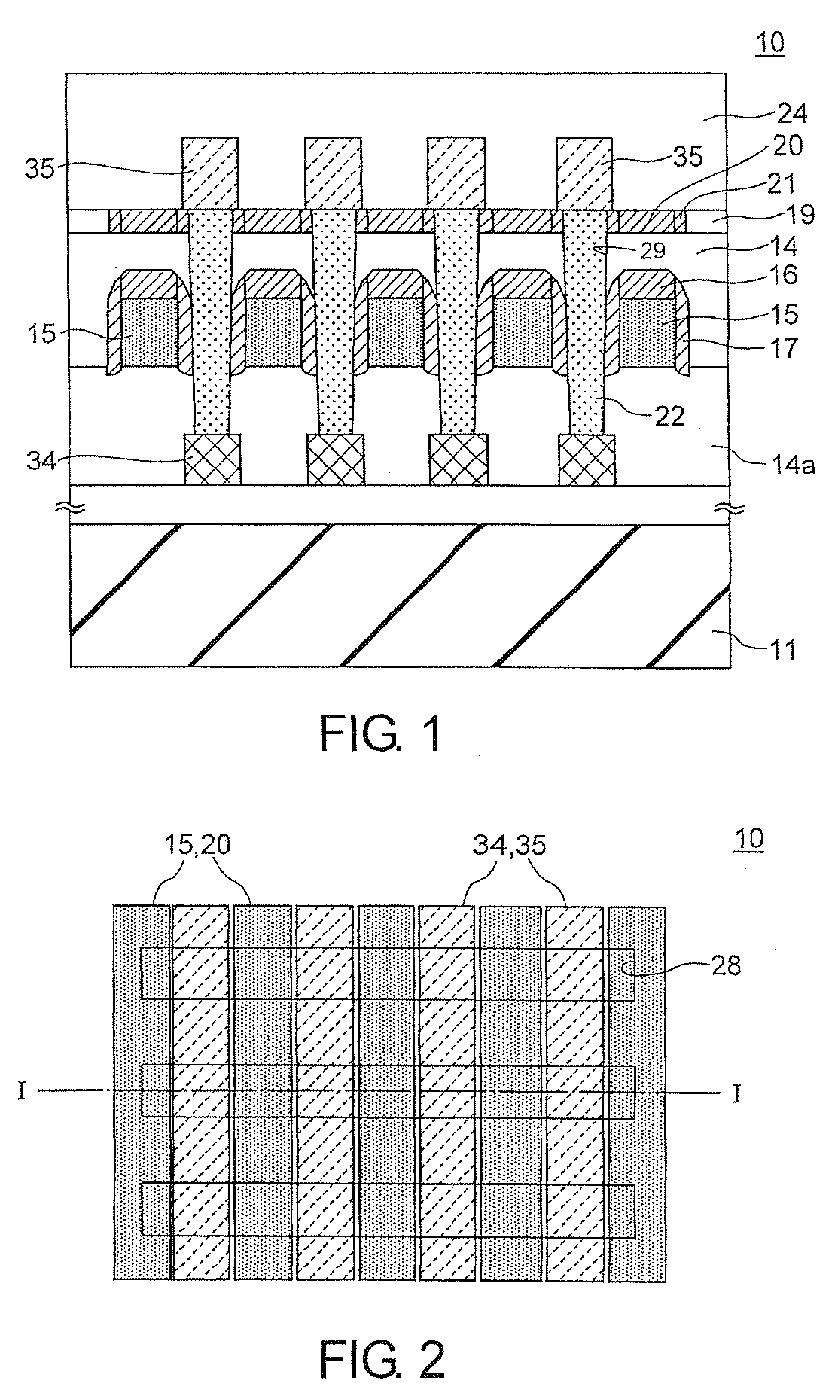
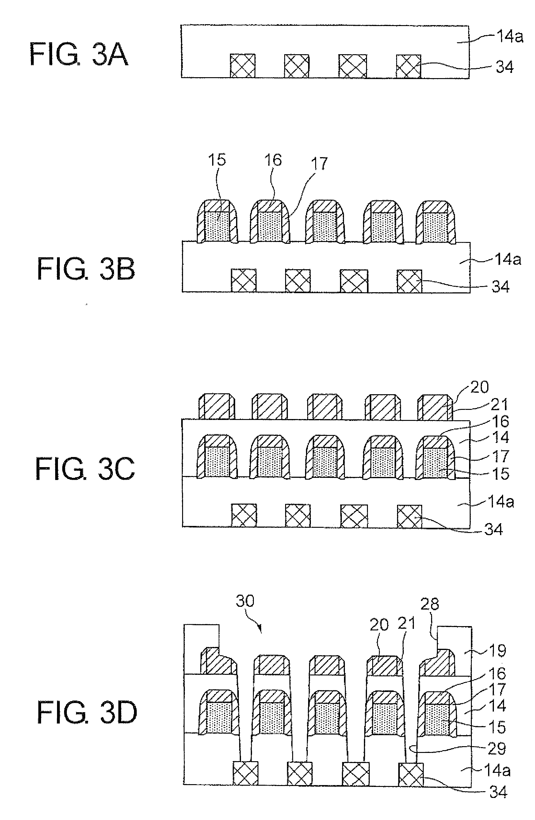
[0028]FIG. 1 is a cross-sectional view showing a semiconductor device according to this invention. FIG. 2 shows a pattern layout of this semiconductor device. FIG. 1 is a cross-sectional view taken along the line I-I of FIG. 2.
[0029]As shown in FIGS. 1 and 2, a semiconductor device 10 has a semiconductor substrate 11, first to third wiring layers 34, 15 and 35 formed on top of the semiconductor substrate 11, first to fourth interlayer insulation films 14a, 14, 19, and 24 for insulating between these wiring layers, dummy mask layers 20 and 21 interposed between the second interlayer insulation film 14 and the fourth interlayer insulation film 24 and formed above wiring lines of the second wiring layer 15, and via plugs 22 for connecting the first wiring layer 34 and the third wiring layer 35. Each of the via plugs 22 passes through between two adjacent wiring lines of the second wiring layer 15.
[0030]Each of the wiring lines of the second wiring layer 15 is provided with a silicon ni...
third embodiment
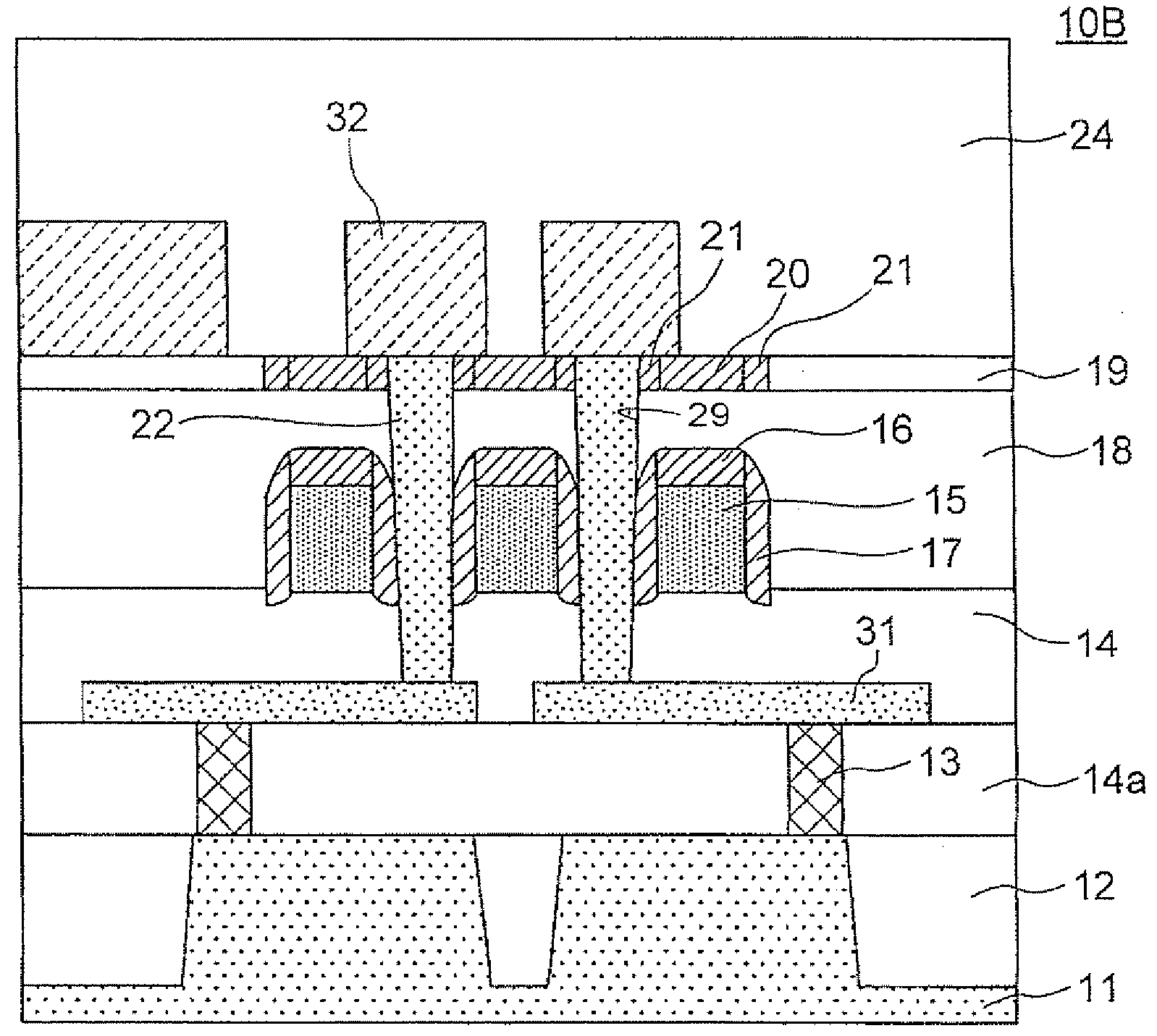
[0046]FIG. 9 is a cross-sectional view showing a semiconductor device according to a third exemplary embodiment of this invention. Like FIG. 2 and so on, FIG. 10 shows a layout pattern of the semiconductor device of this third embodiment, FIG. 9 is a cross-sectional view taken along the line IX-IX of FIG. 10.
[0047]The semiconductor device according to the third embodiment relates to a case in which the configuration of this invention is applied to a logic circuit. In the logic circuit, a first wiring layers 31, a second wiring layer 15 and a third wiring layer 32 are illustrated. These wiring layers may be formed of a material such as tungsten, aluminum, or copper. The semiconductor device 10B is manufactured by a process as described below. Firstly, element isolation regions 12 are formed to define active regions on a semiconductor substrate 11 by a STI process used in a conventional manufacturing process of semiconductor devices. Then, a MISFET (not shown) having a source / drain di...
fourth embodiment
[0057]The input / output device 150 may be a display device such as a liquid crystal display. The storage device 140 other than the semiconductor storage device may be a hard disk or an MO drive. However, this invention is not limited to these. The input / output device 150 may be either one of input and output devices. The semiconductor storage device 120 is for example a RAM (Random Access Memory) or a ROM (Read Only Memory), and is more specifically, a DRAM such as a SRAM (Static Random-Access-Memory), a SDRAM (Synchronous Dynamic Random-Access-Memory), a DDR-SDRAM (Double Data Rate Synchronous Dynamic Random-Access-Memory), a DDR2-SDRAM (Double Data Rate 2 Synchronous Dynamic Random-Access-Memory), or a DDR3-SDRAM (Double Data Rate 3 Synchronous Dynamic Random-Access-Memory), or a storage medium formed by a semiconductor element such as a flash memory. Although only one each of the components of the system is shown in FIG. 11 for the sake of simplification, the numbers of the compon...
PUM
 Abstract
Description
Claims
Application Information