Composition for forming inorganic pattern and method for forming inorganic pattern using the same

a technology of inorganic pattern and composition, which is applied in the field of composition a method for forming inorganic pattern, can solve the problems that the soft lithography method does not convey any more functionality and the method has not been reported as satisfactory, so as to prevent degeneration or precipitation

Inactive Publication Date: 2009-10-15
SAMSUNG ELECTRONICS CO LTD
View PDF9 Cites 6 Cited by
  • Summary
  • Abstract
  • Description
  • Claims
  • Application Information

AI Technical Summary

Benefits of technology

[0009]The composition prepared from these precursors is capable of readily forming an inorganic pattern at a low production cost.
[0015]The method is capable of providing patterned devices with excellent processability and cost reduction.
[0017]The inorganic precursor may be a metal alkoxide or composite metal alkoxide. The stabilizer is added to prevent degeneration or precipitation of the inorganic precursor, and may include, for example, β-diketones such as benzoylacetone and acetylacetone, and β-ketoesters such as methyl acetoacetate, ethyl acetoacetate, isopropyl acetoacetate, and isobutyl acetoacetate.

Problems solved by technology

However, due to intrinsic limitations of these organic materials, soft lithography methods do not convey any more functionality than to serve as an intermediate step of pattern transfer.
However, reports of satisfactory results for the method have not been found, likely due to the numerous technical limitations.

Method used


Image

  • Composition for forming inorganic pattern and method for forming inorganic pattern using the same
  • Composition for forming inorganic pattern and method for forming inorganic pattern using the same
  • Composition for forming inorganic pattern and method for forming inorganic pattern using the same

Examples


example 1

Formation of ZnO Pattern

[0064]1.5 mmol of zinc 2-methoxyethoxide was mixed with an equimolar amount (1.5 mmol) of benzoylacetone under a dry atmosphere with a relative humidity (“RH”) of less than 5%. 0.5 mL of the resulting mixture was then mixed with 2.5 mL of IPA as a solvent to prepare a composition for forming an inorganic pattern. The reaction mixture was spin-coated on a silicon substrate with Cr deposited to a thickness of 100 nm as an electrode, 2 V / μm of a DC electric field was applied between the silicon substrate and an Au-coated upper electrode placed over the Cr electrode so as to leave a gap between the reaction mixture layer and the Au electrode, and the substrate was allowed to stand at room temperature for 1 hour such that the applied dielectric composition formed a pattern with regular spacing. The patterned lower (i.e., Cr) substrate was annealed at 500° C. for 3 hours under atmospheric pressure to convert the zinc precursor into ZnO, followed by removal of resid...

example 2

Formation of TiO2 Pattern

[0065]5 mmol (0.85 mL) of titanium (IV) butoxide was mixed with 2.5 mmol (0.41 g) of benzoylacetone under an atmosphere with an RH of less than 5%, to which 15 mL of pentanol and 2.5 mL of methanol were then added. 5 mmol (based on Ti) of the resulting titanium (IV) butoxide solution was then mixed with an equimolar amount of methyl acetoacetate, and 8 ml of pentanol was then added thereto to prepare a composition for forming an inorganic pattern. Analogously to Example 1, a pattern was formed by electrohydrodynamic lithography. 20 V / μm of an electric field was applied between two substrates, and formation of the pattern was observed while maintaining the electric field for 2.5 hours. After formation of the pattern, annealing was carried out to remove residual solvent and organics at 500° C. for 3 hours under a hydrazine gas atmosphere, resulting in formation of TiO2 pattern. After an electric field was applied during formation of the TiO2 pattern, microscop...

example 3

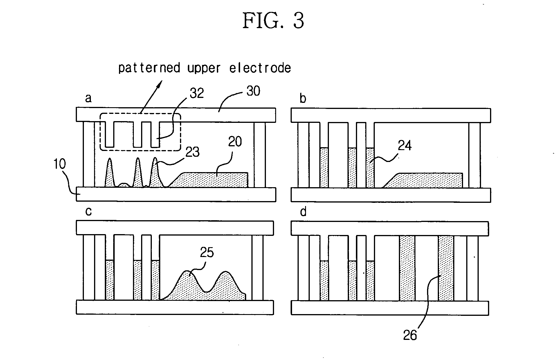
Formation of TiO2 Pattern Using Patterned Upper Electrode

[0066]A pattern was formed in the same manner as in Example 2, except that a patterned conductive Au thin film as shown in FIG. 6a was used as an upper electrode. A microscopic image of the replicated pattern is shown in FIG. 6b.


PUM

PropertyMeasurementUnit
DC electric fieldaaaaaaaaaa
frequencyaaaaaaaaaa
temperatureaaaaaaaaaa

Abstract

Disclosed herein is a composition for forming an inorganic pattern, comprising an inorganic precursor, at least one stabilizer selected from β-diketone and β-ketoester, and a solvent. Use of the composition enables efficient and inexpensive formation of an inorganic micropattern.

Description

[0001]This non-provisional application claims priority to Korean Patent Application No. 10-2008-0034165, filed on Apr. 14, 2008, and all the benefits accruing therefrom under U.S.C. §119, the content of which is incorporated herein by reference in its entirety.BACKGROUND OF THE INVENTION[0002]1. Field of the Invention[0003]This disclosure is directed to a composition for forming an inorganic pattern and a method for forming an inorganic pattern using the same. More specifically, this disclosure is directed to a composition for forming an inorganic pattern, comprising an inorganic precursor, at least one stabilizer selected from β-diketone and β-ketoester, and a solvent, and to a method for forming an inorganic pattern using the same.[0004]2. Description of the Related Art[0005]With advanced semiconductor technology, conventional microstructure fabrication techniques, in particular photolithography (also referred to as “optical lithography”) has with constant advances in optics and m...

Claims


Application Information

Patent Timeline
Patent Type & Authority Applications(United States)
IPC IPC(8): B32B3/02C25D5/24C25D11/00
CPCB81C1/00031B82Y10/00B82Y40/00Y10T428/24322G03F7/0042Y10T428/24479Y10T428/24942G03F7/0002
Inventor CHA, SEUNG NAMKANG, DAE JOONSONG, BYONG GWON
Owner SAMSUNG ELECTRONICS CO LTD
Why Eureka
Try Eureka