Semiconductor device

a technology of semiconductor devices and semiconductor devices, which is applied in the direction of transistors, electroluminescent light sources, electric lighting sources, etc., can solve the problems of reducing the voltage barrier at the boundary, affecting the reliability of semiconductor devices provided with such n-channel transistors having multigate structures, and affecting the characteristics of transistors, so as to improve the reliability of semiconductor devices provided with such n-channel transistors. , the effect of improving the reliability of electronic devices provided with semiconductor devices

Active Publication Date: 2009-10-22
SEMICON ENERGY LAB CO LTD
View PDF33 Cites 42 Cited by
  • Summary
  • Abstract
  • Description
  • Claims
  • Application Information

AI Technical Summary

Benefits of technology

[0037]Further, the first insulating film and the second insulating film are inorganic insulating films such as a silicon oxide film, a silicon nitride film, or a silicon oxynitride (SiOxNy) film. Such an inorganic insulating film can protect the light emitting element compared with an organic insulating film from moisture and oxygen which is considered to cause deterioration of the light emitting element.
[0038]By applying the present invention, an n-channel transistor having a multigate structure in which OFF-state current is reduced and the characteristics of the transistor are improved can be provided. Further, reliability of the semiconductor device provided with such an n-channel transistor having a multigate structure can be improved. In addition, reliability of an electronic device provided with a semiconductor device can be improved. Note that OFF-state current is a leakage current which flows when a polarity of an electric potential by which an inversion layer is not formed is applied to a transistor. Moreover, in the case where the transistor is used as a switching element, OFF-state current also means a current which flows in a location where no current should flow. Further, in accordance with the present invention, characteristic defects of a p-channel transistor (specifically, knot-like characteristic defects generated in a rising portion of an Id-Vg curve) can be suppressed.
[0039]Further, by applying the present invention in which a top end portion of a wiring is covered with an inorganic insulating film a film thickness of 300 nm or less, display defects called dark points which are caused due to a residue generated in forming a wiring when manufacturing a light-emitting display device can be reduced. Note that, the display defects called dark points means pixels of which luminance is reduced compared with other pixels when desired luminance cannot be obtained display is performed by a light-emitting display device.

Problems solved by technology

This results from reduction of voltage barrier at a boundary between the source region and the channel region due to drain voltage, which is caused as the channel length is shortened.
When the short channel effect occurs in any channel region of a transistor having a multigate structure, characteristics of the transistor are impaired.
In particular, when the short channel effect occurs in a source region adjacent to a source electrode, characteristics of the transistor are impaired.

Method used


Image

  • Semiconductor device
  • Semiconductor device
  • Semiconductor device

Examples


embodiment mode 1

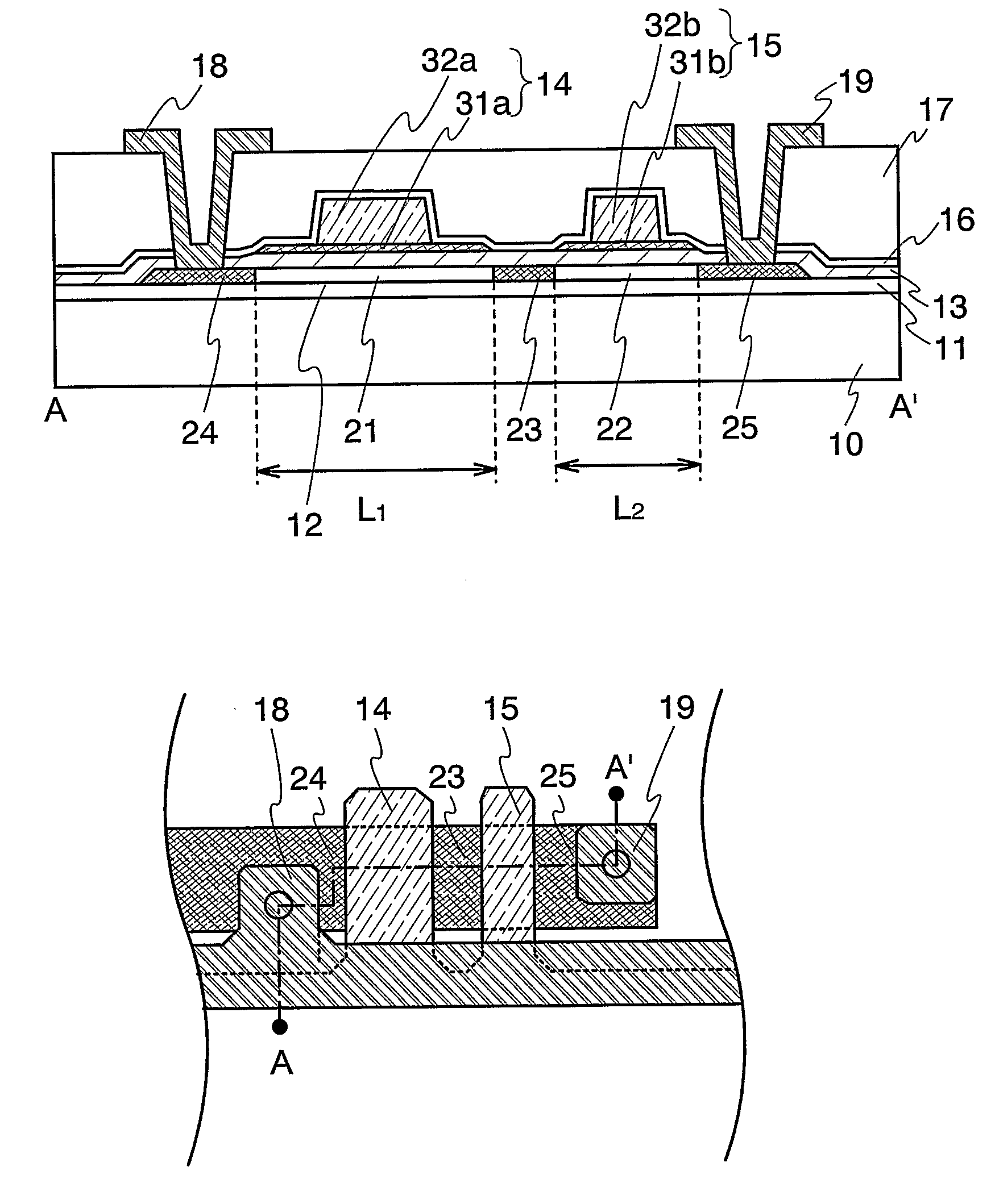
[0062]The present invention relates to a transistor having a multigate structure. A thin film transistor (abbreviation: TFT) is used as a transistor hereinafter. An embodiment mode of the present invention will be described in details with reference to FIGS. 1A and 1B.

[0063]FIG. 1A is a cross-sectional view illustrating an example of a TFT having a multigate structure. FIG. 1B shows a schematic view of the top face of the TFT. Note that the cross-section taken along chain line A-A′ in FIG. 1B corresponds to a cross-sectional view of FIG. 1A. In this embodiment mode, an example of a TFT having two gate electrodes and two channel regions connected in series will be described.

[0064]In a TFT of the present invention, a first insulating film 11 is formed over a substrate 10 and a semiconductor layer 12 is formed over the first insulating film 11. A second insulating film 13 is formed over the semiconductor layer 12 and two gate electrodes are formed over the second insulating film 13. A ...

embodiment mode 2

[0077]In this embodiment mode, examples of methods of manufacturing TFTs having multigate structures of the present invention will be described with reference to FIGS. 2A to 2D and FIG. 3A to 3C.

[0078]First, first insulating film 101 is formed over a substrate 100 having an insulating surface. As the substrate 100, a light-transmitting substrate, for example, a glass substrate, a crystallized glass substrate, or a plastic substrate (polyimide, acrylic, polyethylene terephthalate, polycarbonate, polyarylate, polyethersulfone, or the like) can be used. When a thin film transistor to be formed later is applied to a top-emission (upward emission) light-emitting display device, or applied to a reflective liquid crystal display device, a ceramics substrate, a semiconductor substrate, a metal substrate (tantalum, tungsten, molybdenum, or the like), and the like can also be used. Any substrate can be used as long as it resists at least heat generated in processes.

[0079]As the first insulati...

embodiment mode 3

[0111]In this embodiment mode, a case where a semiconductor layer includes an LDD region will be explained with reference to FIGS. 4A and 4B. Since the components except for a semiconductor layer are the same as Embodiment mode 1 or Embodiment mode 2, the description will not be repeated.

[0112]A semiconductor layer of a TFT of this embodiment mode which is shown in FIG. 4A includes two channel regions placed in series (a first channel region 401 and a second channel region 402); a high concentration impurity region 403 placed between the two channel regions; a source region 404 and a drain region 405 placed under areas outside the two gate electrodes (a first gate electrode and a second gate electrode) over a second insulating film, a pair of first LDD regions 406a and 406b respectively placed between the source region 404 and the first channel region 401 and between the first channel region 401 and the high concentration impurity region 403; and a pair of second LDD regions 407a an...


PUM


Abstract

It is an object to provide a transistor having a new multigate structure in which operating characteristics and reliability are improved. In a transistor having a multigate structure, which includes two gate electrodes electrically connected to each other and a semiconductor layer including two channel regions connected in series formed between a source region and a drain region, and a high concentration impurity region is formed between the two channel regions; the channel length of the channel region adjacent to the source region is longer than the channel length of the channel region adjacent to the drain region.

Description

TECHNICAL FIELD[0001]The present invention relates to a semiconductor device that has a circuit composed of thin film transistors. For example, the present invention relates to an electronic device equipped with, as a component, a display device having an electro-optical device typified by a liquid crystal display panel or an organic light-emitting display device (EL: Electroluminescent device) that has an organic light-emitting element.[0002]It is to be noted that a semiconductor device in this specification refers to general devices that can operate by utilizing semiconductor properties, and such semiconductor devices include all electro-optical devices, semiconductor circuits, and electronic devices.BACKGROUND ART[0003]In recent years, a technique of making thin film transistors (TFTs) using a semiconductor thin film (on the order of several to several hundreds nanometers in thickness) formed over a substrate having an insulating surface has been attracting attention. The thin fi...

Claims


Application Information

Patent Timeline
Patent Type & Authority Applications(United States)
IPC IPC(8): H01L33/00H01L29/786H05B44/00
CPCH01L27/12H01L27/283H01L29/78696H01L29/78645H01L29/42384H10K19/10H10K59/1213H01L27/124
Inventor SAKAKURA, MASAYUKIYAMAZAKI, SHUNPEI
Owner SEMICON ENERGY LAB CO LTD
Why Eureka
Try Eureka