

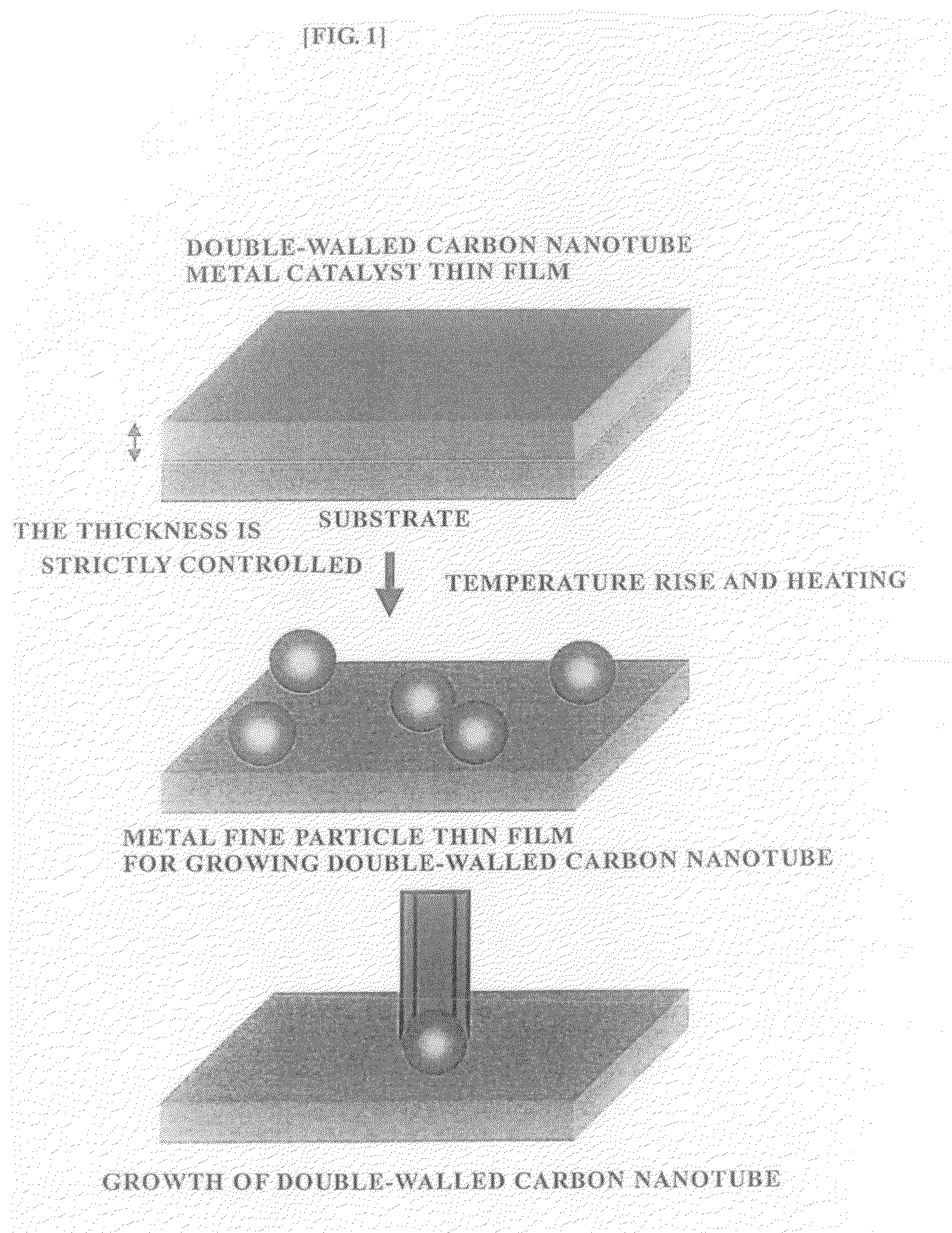
Double-Walled Carbon Nanotube, Aligned Double-Walled Carbon Nanotube Bulk Structure and Process for Producing the Same
a carbon nanotube and double-walled technology, applied in the direction of catalyst activation/preparation, metal/metal-oxide/metal-hydroxide catalyst, chemical vapor deposition coating, etc., can solve the problem of low yield and alignment properties, difficulty in precise control during catalyst adjustment, and insufficient progress in the development of selective production process and formation of bulk structure. , to achieve the effect of high purity, easy control of alignment and growth, and excellent electron emission characteristics
- Summary
- Abstract
- Description
- Claims
- Application Information
AI Technical Summary
Benefits of technology
Problems solved by technology
Method used
Image

Examples
example 1
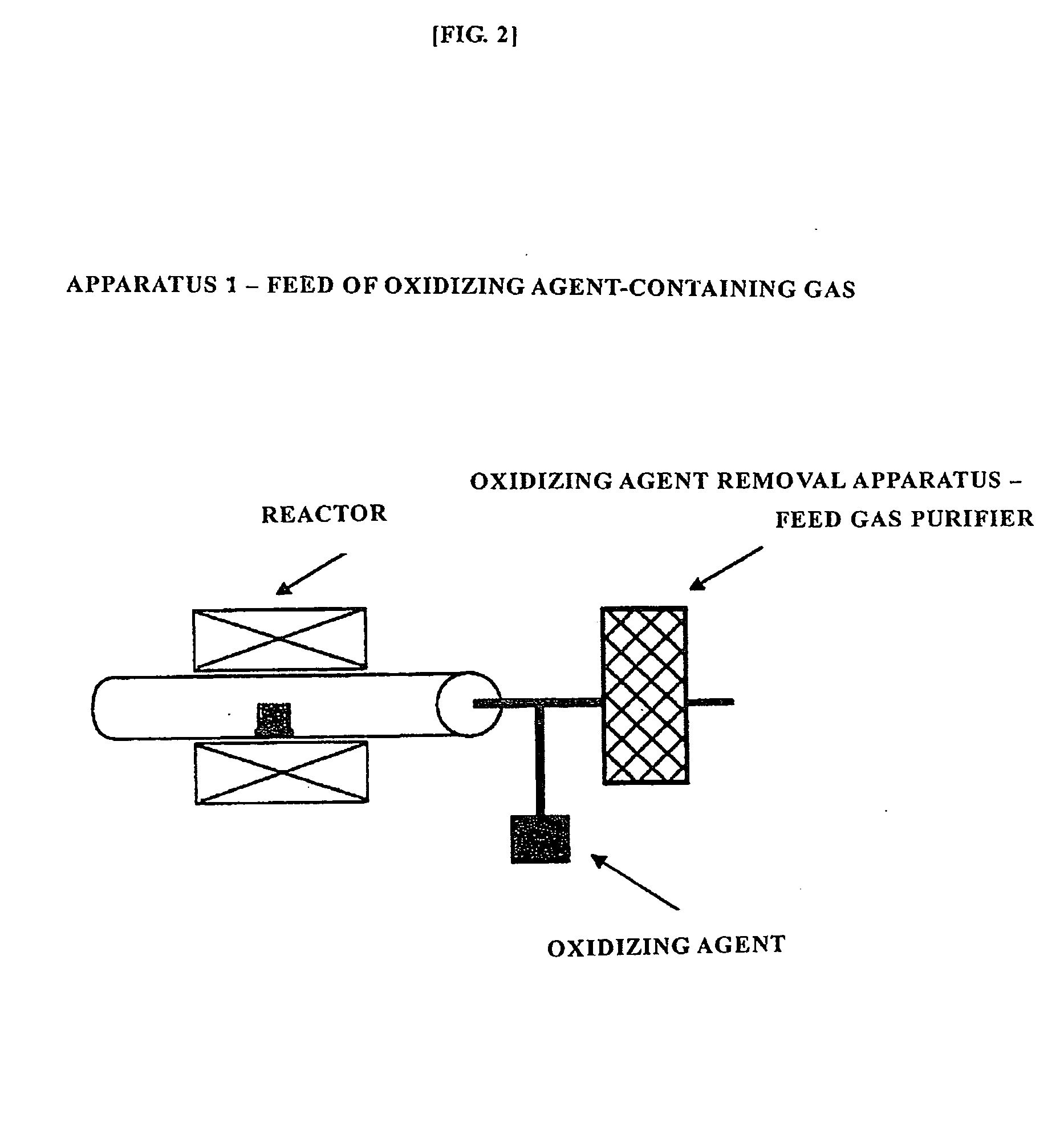
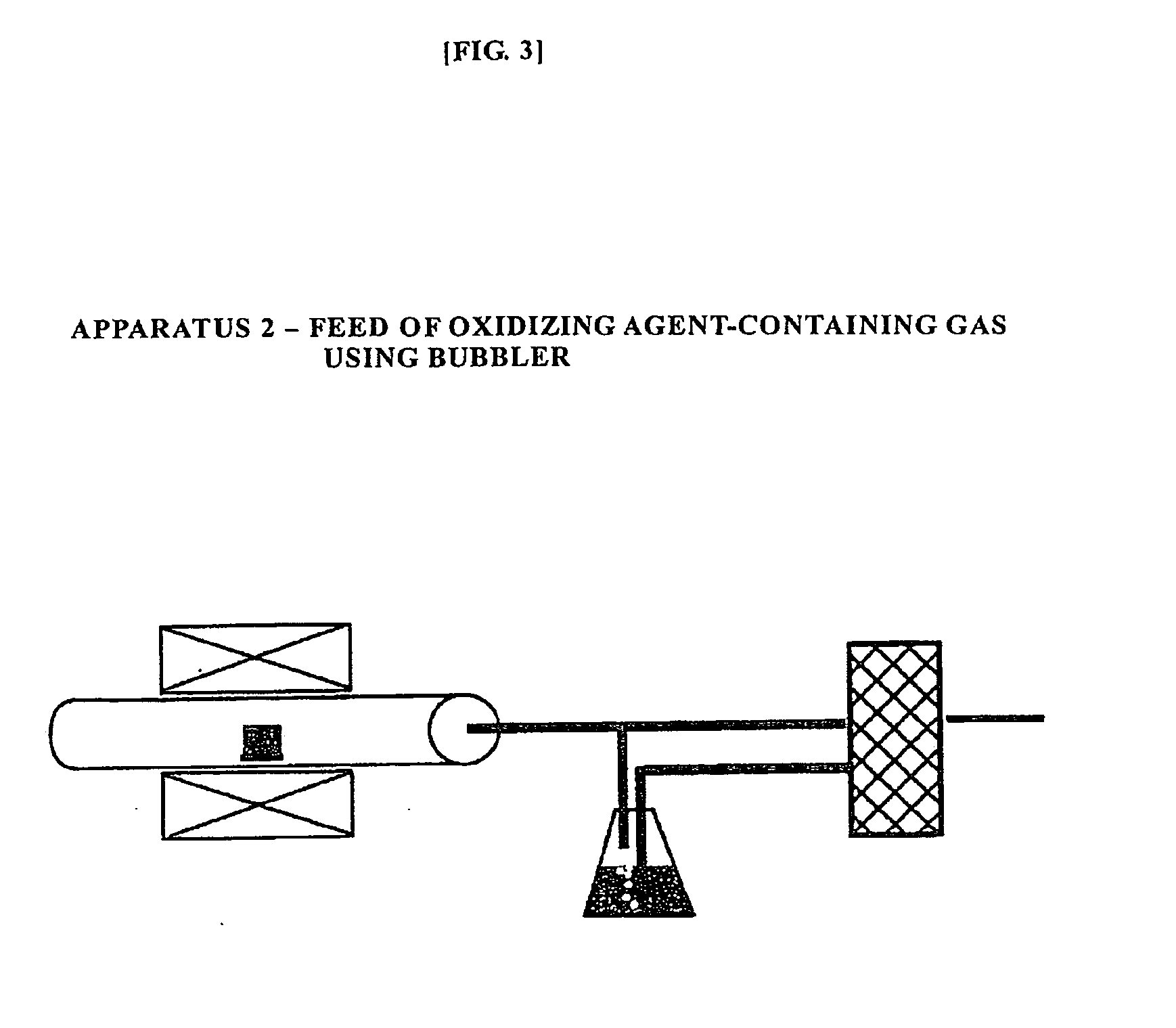
[0161]A carbon nanotube was grown by the CVD method under the following condition.
[0162]Carbon compound: Ethylene, feed rate at 200 sccm
[0163]Atmospheric (gas) (Pa): Helium and hydrogen mixed gas, feed rate at 2,000 sccm
[0164]Pressure: Atmospheric pressure
[0165]Addition amount of water vapor (ppm): 300 ppm
[0166]Reaction temperature (° C.): 750° C.
[0167]Reaction time (min): 30 minutes
[0168]Metal catalyst (existence amount): Iron thin film, 1.69 nm in thickness
[0169]Substrate: Silicon wafer
[0170]The catalyst was disposed on the substrate using a sputtering vapor deposition apparatus and vapor deposited.
[0171]FIG. 10 exemplifies an external appearance of a vertically aligned double-walled carbon nanotube bulk structure obtained through the growth under the foregoing condition. In the drawing, the near side shows a ruler. The vertically double-walled carbon nanotube film having a height of 2.2 mm grows on the silicon wafer in the bottom. An SEM image of a vertex of this film is shown in...
example 2
[0173]A carbon nanotube was grown by the CVD method under the following condition.
[0174]Carbon compound: Ethylene, feed rate at 100 sccm
[0175]Atmospheric (gas) (Pa): Helium and hydrogen mixed gas, feed rate at 1,000 sccm
[0176]Pressure: Atmospheric pressure
[0177]Addition amount of water vapor (ppm): 300 ppm
[0178]Reaction temperature (° C.): 750° C.
[0179]Reaction time (min): 10 minutes
[0180]Metal catalyst (existence amount): Iron thin film, 1.69 nm in thickness
[0181]Substrate: Silicon wafer
[0182]The catalyst was disposed on the substrate by sputtering vapor deposition.
[0183]FIGS. 12 to 14 are each a photographic image obtained by peeling off the vertically aligned double-walled carbon nanotube prepared in Example 2 from the substrate using a pair of tweezers, dispersing it in a solution, placing it on a grid of an electron microscope (TEM) and observing it by an electron microscope (TEM). It is noted that neither the catalyst nor amorphous carbon is incorporated in the obtained carbon...
example 3
[0187]A carbon nanotube was grown by the CVD method under the following condition.
[0188]Carbon compound: Ethylene, feed rate at 100 sccm
[0189]Atmospheric (gas): Helium and hydrogen mixed gas, feed rate at 1,000 sccm
[0190]Pressure: Atmospheric pressure
[0191]Addition amount of water vapor (ppm): 300 ppm
[0192]Reaction temperature (° C.): 750° C.
[0193]Reaction time (min): 10 minutes
[0194]Metal catalyst (existence amount): Iron thin film, 0.94, 1.32, 1.62, 1.65, 1.69 and 1.77 nm in thickness
[0195]Substrate: Silicon wafer
[0196]The catalyst having each thickness was disposed on the substrate by sputtering vapor deposition.
[0197]FIG. 17 shows the relationship of a thickness of each iron film and a center of outer diameter distribution of the carbon nanotube; and the proportions (%) of single-walled, double-walled and triple-walled or multi-walled nanotubes are shown in the following Table 1.
TABLE 1Thickness ofDouble-walledSingle-walledMulti-wallediron film [nm][%][%][%]0.948.5987.14.291.321...
PUM
| Property | Measurement | Unit |
|---|---|---|
| outer diameter | aaaaa | aaaaa |
| outer diameter | aaaaa | aaaaa |
| thickness | aaaaa | aaaaa |
Abstract
Description
Claims
Application Information