Donor substrate and method of manufacturing display

Inactive Publication Date: 2009-12-31
SONY CORP
View PDF0 Cites 29 Cited by
  • Summary
  • Abstract
  • Description
  • Claims
  • Application Information

AI Technical Summary

Benefits of technology

[0024]In the first donor substrate according to the embodiment of the present invention, a heat interfering layer including two or more layers with refraction index different from each other is arranged between the base and the photothermal conversion layer. Thereby, reflectance of the heat interfering layer is adjusted depending on a light emission band of the radiation ray, and absorption when the radiation ray irradiated to the donor substrate is absorbed in the photothermal conversion layer and converted into heat is improved.
[0025]In the second donor substrate according to the embodiment of the present invention, the pollution preventing layer includes a first portion formed on a top surface of the convex structure and a second portion formed on a top surface of the heat insulating layer, and the first portion and the second portion are separated from each other. Thus, heat diffusion through the pollution preventing layer is highly reduced. Thereby, a risk that an undesired range in the transfer layer is transferred is reduced, and a desired range is transferred with high ac

Problems solved by technology

However, in the case of thermal transfer by using laser, when size of the substrate is increased, there is an issue that processing time is extended and cost of the display or the like is up.
However, a donor substrate capable of efficiently absorbing a radiation ray with a wide wavelength such as a flash lamp

Method used


Image

  • Donor substrate and method of manufacturing display
  • Donor substrate and method of manufacturing display
  • Donor substrate and method of manufacturing display

Examples


first embodiment

Display

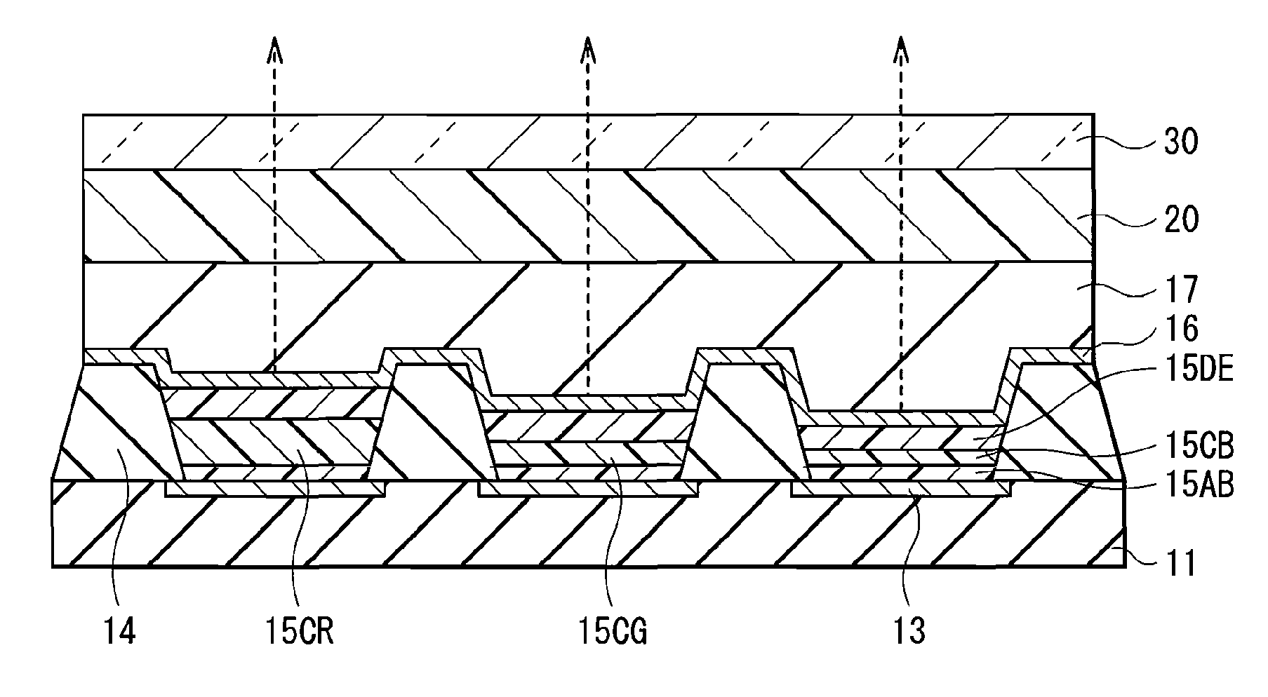
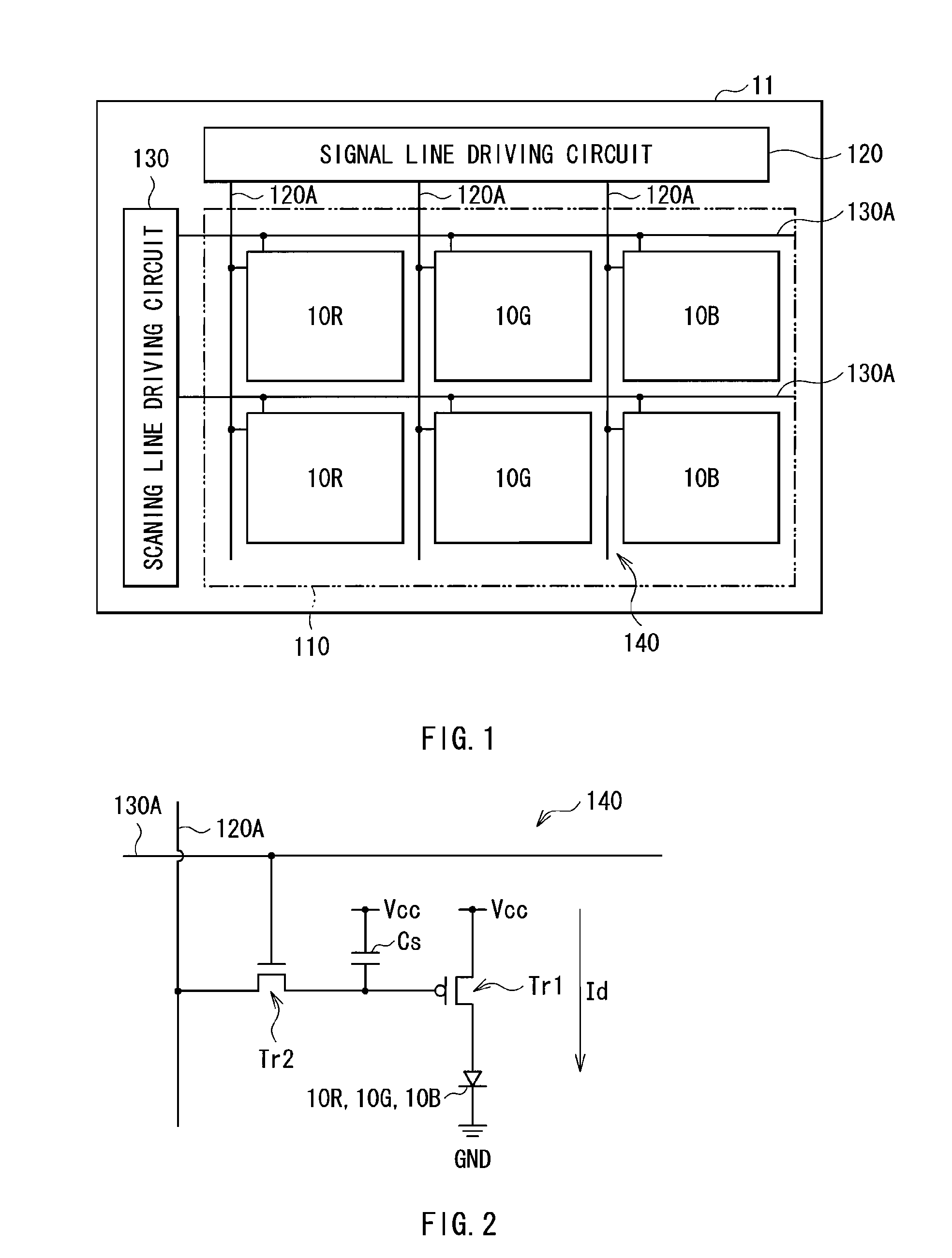
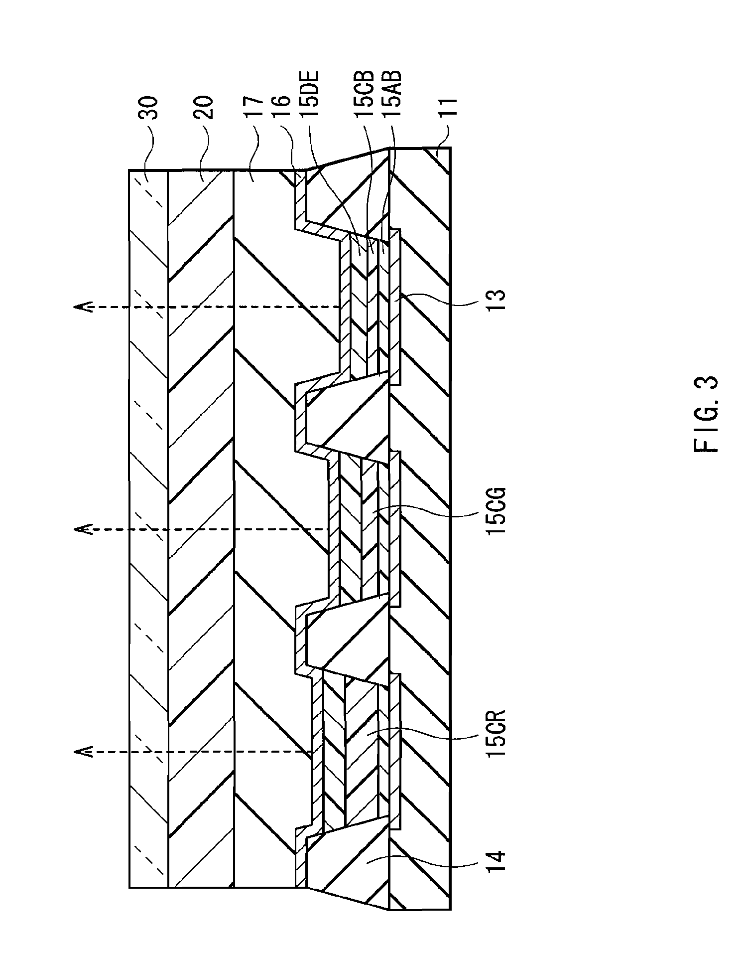
[0063]FIG. 1 illustrates the configuration of a display according to a first embodiment of the present invention. The display is used as a low-profile organic light emitting color display or the like. In the display, for example, a display region 110 in which a plurality of light emitting devices 10R, 10G, and 10B which will be described later are arranged in matrix is formed on a driving substrate 11 of glass, and a signal line driving circuit 120 and a scanning line driving circuit 130 as drivers for image display are formed in vicinity of the display region 110.

[0064]In the display region 110, a pixel driving circuit 140 is formed. FIG. 2 illustrates an example of the pixel driving circuit 140. The pixel driving circuit 140 is formed in a layer level below that of a first electrode 13 which will be described later. The pixel driving circuit 140 is an active driving circuit including a driving transistor Tr1 and a writing transistor Tr2, a capacitor Cs (retention capacity) ...

modification 1

[0113]FIG. 11 illustrates the configuration of a donor substrate 40A according to Modification 1 of the present invention. In the donor substrate 40A in Modification 1, a photothermal conversion layer 42 is provided for each region separated with a convex structure 44. Thereby, it is possible that a transfer layer containing light emission material of different colors for each region is formed, and the number of transfers is reduced. Except the above, the configuration is the same as the first embodiment.

[0114]The donor substrate 40A in Modification 1 may be manufactured in the same manner as in the first embodiment except that the photothermal conversion layer 42 is provided for each region separated with the convex structure 44.

[0115]Next, a method of manufacturing a display using the donor substrate 40A of Modification 1 will be described.

[0116]Similarly to the first embodiment, a first electrode 13, an insulating layer 14, and a hole injecting layer and a hole transporting layer...

second embodiment

[0122]FIG. 14 illustrates the configuration of a donor substrate 40B according to a second embodiment of the present invention. The donor substrate 40B has the same configuration as the donor substrate 40 in the first embodiment except that a heat interfering layer 46 is provided between a base 41 and a photothermal conversion layer 42. Therefore, same reference numerals are used to indicate substantially identical components, and the descriptions are omitted.

[0123]The base 41, the photothermal conversion layer 42, a heat insulating layer 43, a convex structure 44, and a pollution preventing layer 45 are manufactured in the same manner as the first embodiment.

[0124]The heat insulating layer 46 increases absorption of a laser light LB in the photothermal conversion layer 42. The heat insulating layer 46 has, for example, a thickness of 15 nm or more and 80 nm or less, and is made of a-Si. The photothermal conversion layer 42 and the heat interfering layer 46 are arranged correspondin...


PUM

PropertyMeasurementUnit
Thicknessaaaaaaaaaa
Thicknessaaaaaaaaaa
Thicknessaaaaaaaaaa

Abstract

The present invention provides a donor substrate used in forming a light emitting layer by forming a transfer layer containing light emission material, irradiating a radiation ray to the transfer layer while the transfer layer and a substrate to be transferred face each other, and sublimating or vaporizing the transfer layer so that the transfer layer is transferred to the substrate to be transferred. The donor substrate includes: a base; a photothermal conversion layer arranged on the base; and a heat interfering layer arranged between the base and the photothermal conversion layer, and including two or more layers with refraction index different from each other.

Description

BACKGROUND OF THE INVENTION[0001]1. Field of the Invention[0002]The present invention relates to a donor substrate used in forming a light emitting layer in an organic light emitting device by transfer method, and a method of manufacturing a display using such a donor substrate.[0003]2. Description of the Related Art[0004]In recent years, displays for the next generation have been actively developed, and an organic light emitting display using an organic light emitting device (organic EL (electroluminescence) device) in which a first electrode, a plurality of organic layers including a light emitting layer, and a second electrode are stacked in this order on a driving substrate has attracted attention. Since the organic light emitting display is self-emitting, it has a large view angle. In the organic light emitting display, since a backlight is unnecessary, electric power saving is expected. Moreover, responsiveness is high, and low-profile of the display is possible. Therefore, it...

Claims


Application Information

Patent Timeline
IPC IPC(8): H01J9/00
CPCH01L27/3211Y10S430/146H01L51/56H01L51/0013C23C14/048H10K59/35H10K71/18H10K71/00
Inventor HIGO, TOMOYUKIMATSUO, KEISUKE
Owner SONY CORP
Why Eureka
Try Eureka