Power receiving control device, power receiving device, and electronic apparatus

a power receiving control and power technology, applied in the direction of instruments, inductances, transportation and packaging, etc., can solve the problems of reducing the charging time, power loss, and shortening the charging time of secondary batteries utilizing contactless power transmission, so as to reduce the charging time of secondary batteries, reduce the loss, and simple and small structure

Active Publication Date: 2010-01-21
SAMSUNG ELECTRONICS CO LTD
View PDF3 Cites 55 Cited by
  • Summary
  • Abstract
  • Description
  • Claims
  • Application Information

AI Technical Summary

Benefits of technology

[0051]The present invention is applicable to various electronic devices such as watches, codeless phones, shavers, electric toothbrushes, wrist computers, handy terminals, personal digital assistants, and electric bicycles. Especially, the invention is suitably applied to mobile terminals (including a cell phone unit, a PDA terminal, and a portable personal computer terminal) or watches. The power receiving device of the aspect has a simple and small-sized structure so as to be able to be mounted on mobile terminals or the like. Further, the power receivin

Problems solved by technology

However, they require rigorous charging control with a consideration to deterioration or safety thereof, thus requiring highly-accurate charging control technique.
However, charging efficiency of the secondary battery utilizing the contactless power transmission is lower than that of a normal charger (a charger using an AC adaptor) and therefore the secondary battery utilizing the contactless power transmission tends to require longer charging time.
According to an inspection of the inventor, it became apparent that power loss occurs in the regulator described above to hinder decrease of the charging time in a case requiring flow of a large amount of charging current such as a case of charging a secondary battery with high exhaustion.
It become apparent that, in power supply through the bypass path bypassing the regulator, overshoot and undershoot might occur in a case where power feeding to the load as the power feeding object is temporarily stopped or in a case where the power feeding under the temporal stop is restarted.
Therefore, a voltage at an output node of the regulator rises sharply, causing overshoot.
When the power feeding, which has been temporarily stopped, is restarted, the load rapidly draws great current so as to cause a lack of power supply.
Therefore, the voltage at the output node of the regulator is rapidly decreased, causing undershoot.
Overshoot and undershoot may cause defects such as a damage of a circuit at the secondary side and require of reset of a control IC (for example, a charging device for controlling charge of the secondary battery) for controlling the power feeding to the load.
That is, if a large amount of current is supplied to the load in the modulation of the load of the power receiving device, the primary side has a difficulty to detect change of a voltage, which occurs by the load modulation, at a coil end of the primary coil.
Thus, the primary side has a difficulty to recognize a communication signal produced by the load modulation.
If a foreign object (a thin metal plate, for example) having a large area is inserted between the primary coil and the secondary coil in the normal power transmission from the primary side to the secondary side, the foreign object consumes whole of the power supplied from the primary side.
If the takeover state arises, the foreign object generates heat so as to cause accidents such as device

Method used


Image

  • Power receiving control device, power receiving device, and electronic apparatus
  • Power receiving control device, power receiving device, and electronic apparatus
  • Power receiving control device, power receiving device, and electronic apparatus

Examples


first embodiment

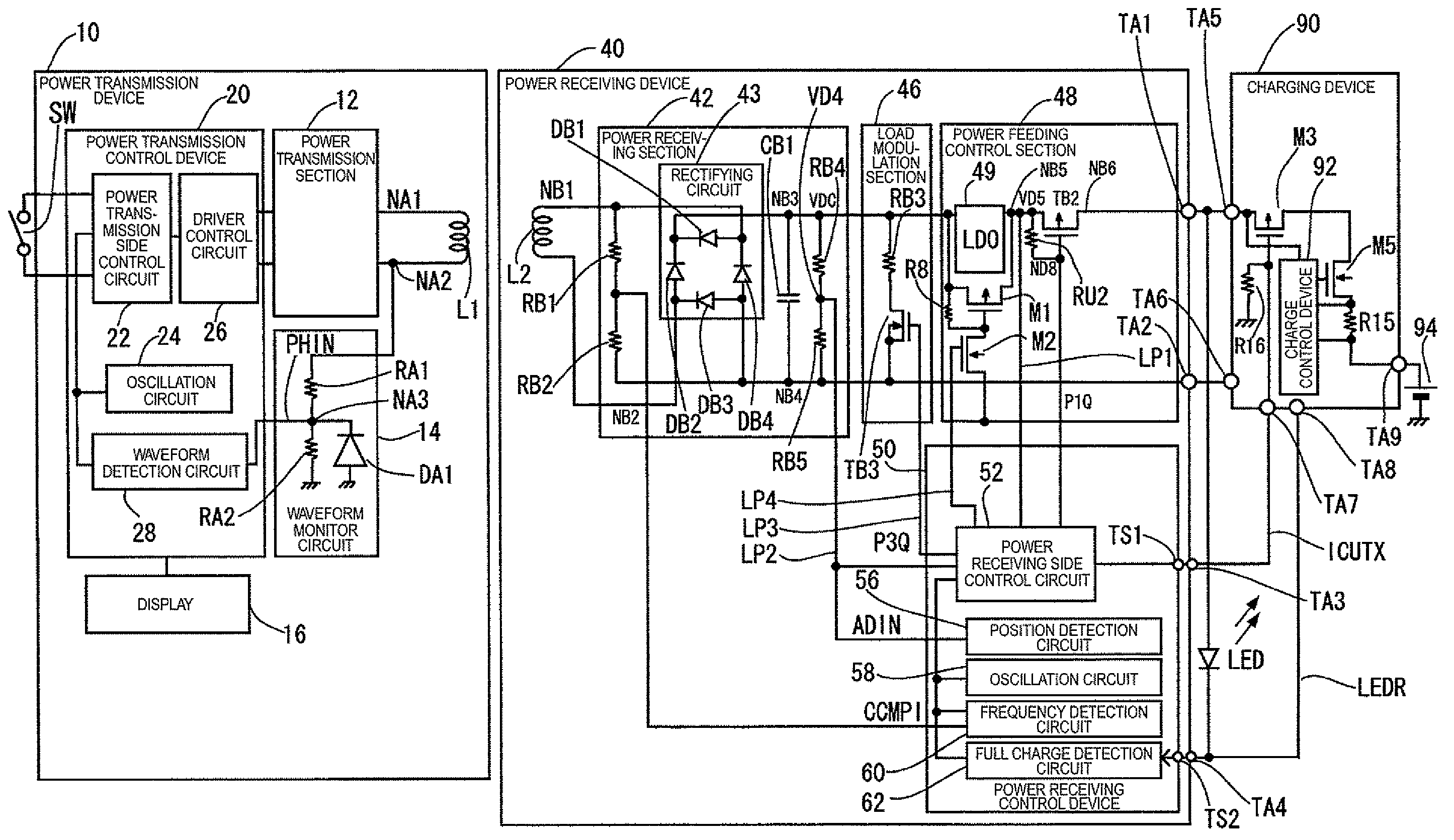
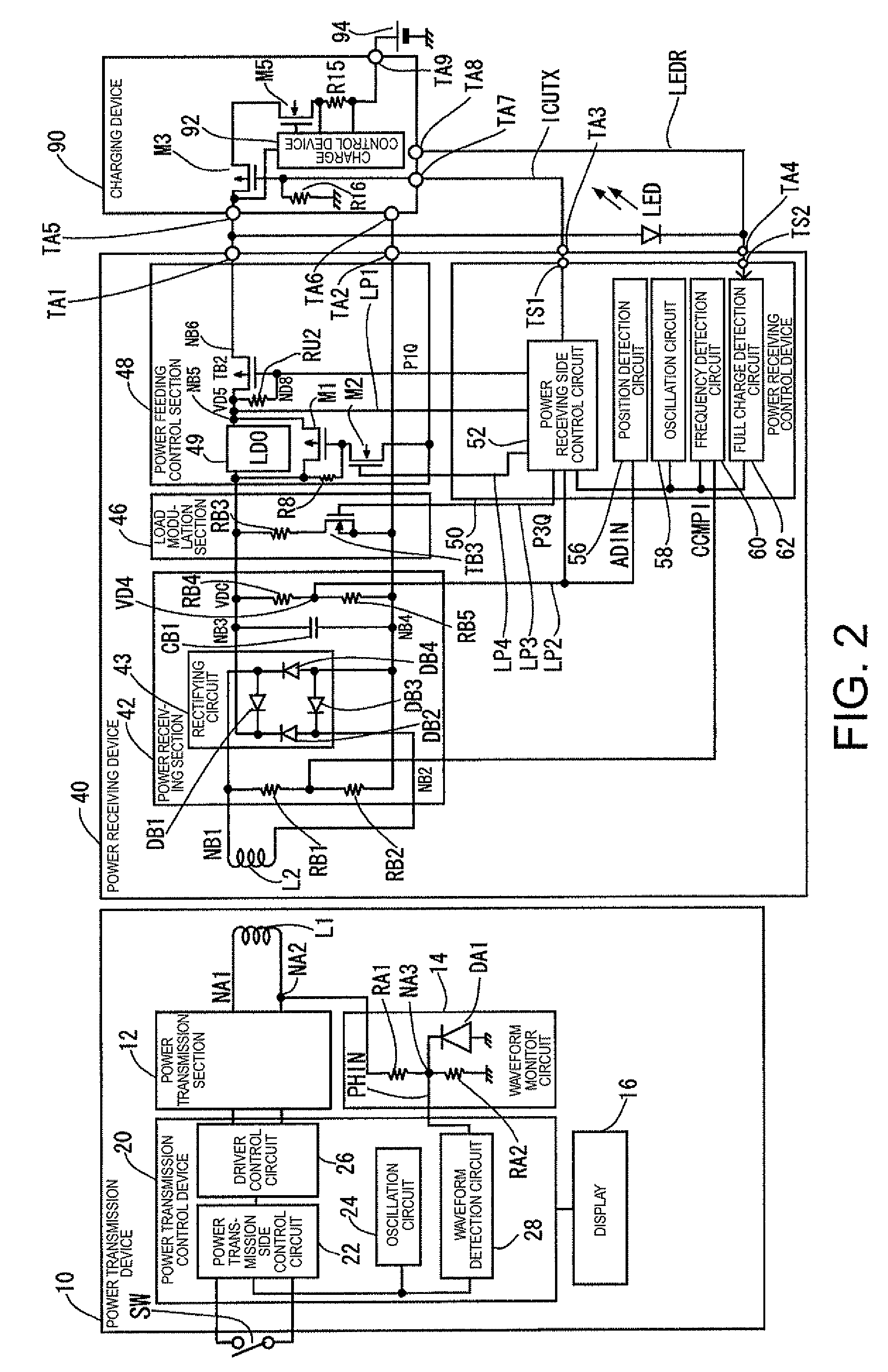
[0071]A contactless power transmission system will now be described.

[0072]Structure of Electronic Apparatus

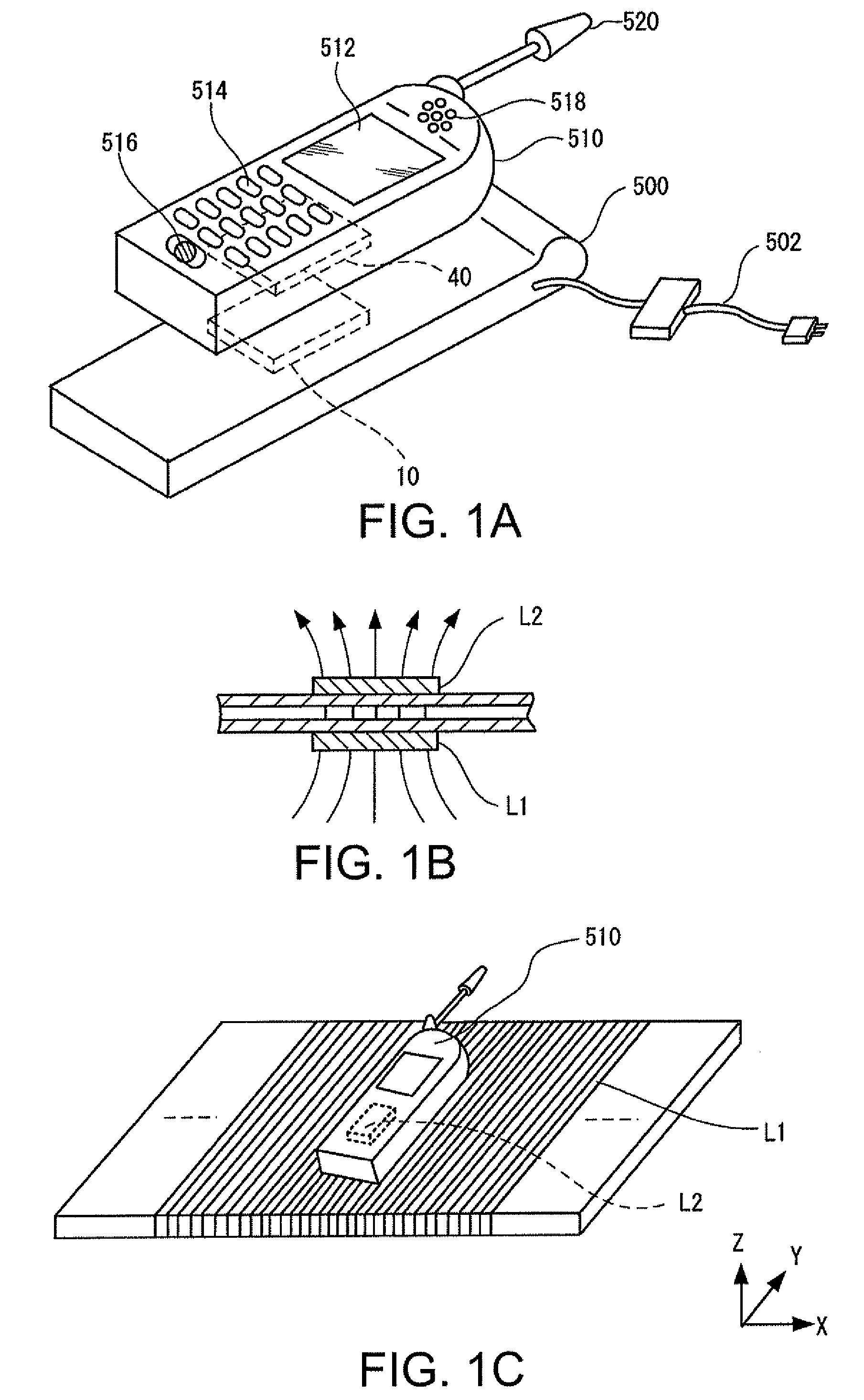
[0073]FIGS. 1A to 1C are diagrams showing an example of a structure of a contactless power transmission system. FIG. 1A shows an example of an electronic apparatus employing a contactless power transmission method according to a first embodiment of the invention. A charger 500 (a cradle) that is one of electronic apparatuses includes a power transmission device 10. A cell phone 510 that is one of electronic apparatuses includes a power receiving device 40. The cell phone 510 includes a display 512 such as a liquid crystal display (LCD), an operation section 514 composed of buttons and the like, a microphone 516 (a sound input section), a speaker 518 (a sound output section), and an antenna 520.

[0074]Power is supplied to the charger 500 through an AC adapter 502, and then the power is transmitted from the power transmission device 10 to the power receiving device 40 by the conta...

second embodiment

[0228]FIG. 16 is a diagram showing a circuit structure of a power receiving side control circuit according to a second embodiment. In the first embodiment, as shown in FIG. 14, the first NMOS transistor MA and the second NMOS transistor MB are simultaneously turned on so as to reset the hysteresis comparator.

[0229]In the second embodiment, as shown in FIG. 16, a reset switch Q10 (composed of a reset transistor MC, for example) is provided in parallel to the first NMOS transistor MA and the second NMOS transistor MB. Further, a resistance value of the resistance R54 is set to be sufficiently smaller than those of the resistances R52 and R53.

[0230]For the reset of the comparator, the reset switch Q10 (the reset transistor MC) is turned on under a state that the first NMOS transistor MA and the second NMOS transistor MB are off. The resistance value of the resistance 54 is small, so that large amount of current flows through the bias current path including the resistances R50, R51, and...


PUM


Abstract

A power receiving control device provided to a power receiving device included in a contactless power transmission system that transmits electric power from a power transmission device to the power receiving device by electromagnetically coupling a primary coil and a secondary coil so as to feed the electric power to a load serving as a power feeding object from a voltage output node of the power receiving device, which includes a rectifying circuit and a regulator; and transmits a load modulation signal to the power transmission device by load modulation performed by a load modulation section included in the power receiving device, in a period of the power feeding to the load as the power feeding object, includes a power receiving side control circuit controlling an operation of the power receiving device; and a power supply control signal output terminal for outputting a power supply control signal by which the power feeding to the load is temporarily stopped In the device, the power receiving side control circuit turns on a switch circuit provided between an input node and an output node of the regulator, based on detection of lowering of power feeding capability to the load, so as to put a bypass path, which directly connecting the input node and the output node of the regulator, in an ON state; turns off the switch circuit so as to forcibly put the bypass path in an OFF state, in a case where the power feeding to the load is temporarily stopped in a period during which the bypass path is formed, at one of timing at which a voltage level of the power supply control signal outputted from the power supply control signal output terminal is switched from a non-active level to an active level so as to temporarily stop the power feeding to the load and timing before the power feeding to the load is temporarily stopped; and turns on the switch circuit after releasing the temporary stop of the power feeding to the load so as to return the bypass path to the ON state.

Description

[0001]The present application claims a priority based on Japanese Patent Application No. 2008-183853 filed on Jul. 15, 2008, the contents of which are incorporated herein by reference.BACKGROUND[0002]1. Technical Field[0003]The present invention relates to a power receiving control device, a power receiving device, and an electronic apparatus.[0004]2. Related Art[0005]In resent years, a contactless power transmission technique, which utilizes electromagnetic induction so as to enable power transmission even without a metallic contact point, has attracted lots of attention. As an application of the contactless power transmission technique, charging of a cell-phone or a household appliance (for example, a cordless handset for a telephone) is proposed.[0006]JP-A-2006-60909, for example, discloses a contactless power transmission device using a primary coil and a secondary coil.[0007]Recently, secondary batteries such as a lithium-ion battery and a lithium polymer battery have been wide...

Claims


Application Information

Patent Timeline
IPC IPC(8): H01F38/14H02J1/00H02J7/00
CPCG08C17/04H02J7/025H01F2038/143H02J50/10H02J7/00034H02J50/80H02J50/90H02J50/60H02J50/12
Inventor ONISHI, KOTAKAMIYAMA, MASAYUKISHIOZAKI, NOBUTAKAYODA, KENTAROKAMIJO, TAKAHIRO
Owner SAMSUNG ELECTRONICS CO LTD
Why Eureka
Try Eureka