Method of synthesizing ITO electron-beam resist and method of forming ITO pattern using the same

a technology of electron beam and indium tin oxide, which is applied in the direction of liquid/solution decomposition chemical coating, instruments, photosensitive materials, etc., can solve the problems of low throughput, inadequacies of wet etching methods for forming nano-scale fine patterns, and contaminating etching baths with exfoliated photoresist patterns, etc., to achieve high optical transmittance and low resistivity

Active Publication Date: 2010-02-11
ELECTRONICS & TELECOMM RES INST
View PDF0 Cites 11 Cited by
  • Summary
  • Abstract
  • Description
  • Claims
  • Application Information

AI Technical Summary

Benefits of technology

[0017]An ITO electron beam resist can be obtained using a method of synthesizing an ITO electron beam resist according to the present invention.
[0018]A method of forming an ITO pattern according to the present invention does not include an etching process or a lift-off process, and thus, the ITO pattern can be formed using a simple process by directly realizing a pattern on an ITO electron beam resist film using an electron beam writer. In the method of forming an ITO pattern according to the present invention, various patterns having a size as small as a few nm can be formed depending on the resolution of the electron beam writer.
[0019]The method of forming an ITO pattern according to the present invention can remove conventional problems, for example, an adhesion problem between a photoresist film and an ITO thin film, a problem of re-deposition of the photoresist, or the problem of realizing a pattern having a size less than 1 μm, which are caused in an etching process or a lift-off process.
[0020]An ITO thin film or an ITO pattern formed using an ITO electron beam resist according to the present invention has optical characteristics of having a high optical transmittance in a visible light region and has electrical characteristics of having very low resistivity.

Problems solved by technology

However, the wet process has drawbacks in that the exfoliation of photoresist pattern occurs during an etching process due to a weak bonding force between the photoresist pattern and the ITO thin film, and the exfoliated photoresist pattern can contaminate an etching bath.
Furthermore, the wet etching method is not appropriate for forming a nano scale fine pattern due to isotropical etching characteristics of the wet etching.
The dry etching method can form a fine pattern of 5 μm or less, however, has a low through-put, and has a problem in which re-depositing of the photoresist occurs during the etching process.
The etching method that uses a laser can form a fine pattern of approximately 1 μm, however, this method is only effective for forming an ITO pattern of a simple matrix stripe shape.

Method used


Image

  • Method of synthesizing ITO electron-beam resist and method of forming ITO pattern using the same
  • Method of synthesizing ITO electron-beam resist and method of forming ITO pattern using the same
  • Method of synthesizing ITO electron-beam resist and method of forming ITO pattern using the same

Examples


Embodiment Construction

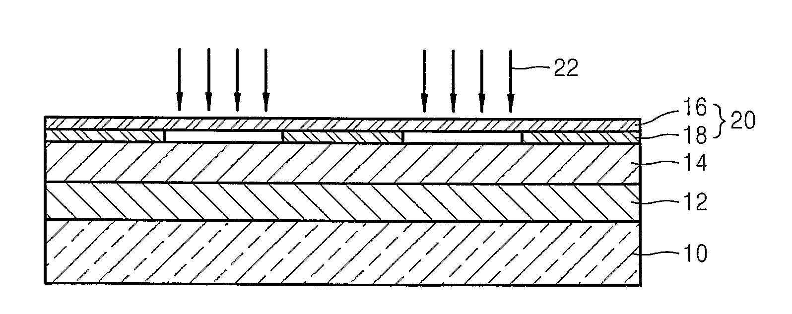
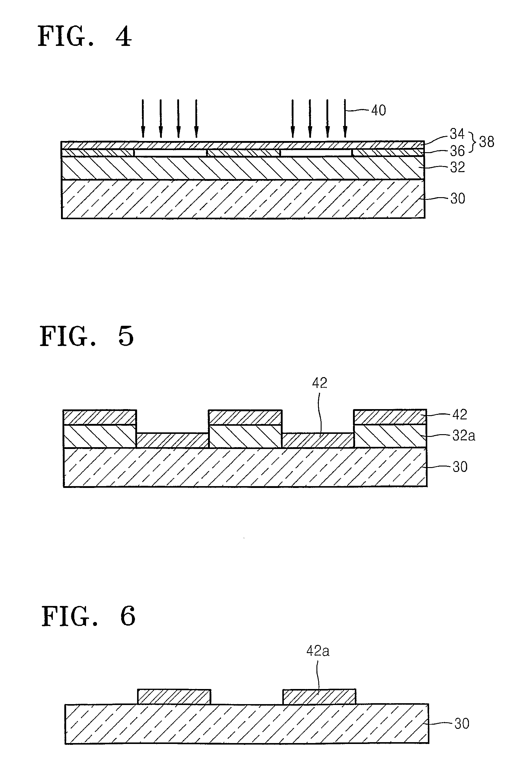
[0032]The present invention will now be described more fully with reference to the accompanying drawings in which exemplary embodiments of the invention are shown. The invention may, however, be embodied in many different forms and should not be construed as being limited to the embodiments set forth herein; rather, these embodiments are provided so that this disclosure will be thorough and complete, and will fully convey the concept of the invention to those skilled in the art. In the drawings, the thicknesses of layers and regions are exaggerated for clarity.

[0033]As described above, in order to address conventional problems caused during forming of an ITO pattern, the present invention does not use a photoresist film, but uses an ITO electron beam resist that reacts with an electron beam. A method of synthesizing the ITO electron beam resist will now be described.

[0034]FIG. 7 is a flow chart for explaining a method of synthesizing an ITO electron beam resist according to the pres...


PUM

PropertyMeasurementUnit
molar ratioaaaaaaaaaa
sizeaaaaaaaaaa
temperatureaaaaaaaaaa

Abstract

Provided is a method of synthesizing an ITO electron beam resist and a method of forming an ITO pattern. The ITO electron beam resist is synthesized by dissolving indium chloride tetrahydrate and tin chloride dihydrate in 2-ethoxy ethanol. The method of forming an ITO pattern includes: forming an ITO electron beam resist film on a substrate, forming an ITO electron beam resist pattern by patterning the ITO electron beam resist film, and forming an ITO pattern by annealing the ITO electron beam resist pattern.

Description

TECHNICAL FIELD[0001]This application claims the benefit of Korean Patent Application No. 10-2007-0026774, filed on Mar. 19, 2007, in the Korean Intellectual Property Office, the disclosure of which is incorporated herein in its entirety by reference. The present invention relates to a method of synthesizing an indium tin oxide (ITO) electron-beam resist and a method of forming an ITO pattern using the method. The present invention is produced as a result of study supported by the IT R&D program of MIC / IITA, [2005-S-605-02, IT-BT-NT Convergent Core Technology for advanced Optoelectronic Devices and Smart Bio / Chemical Sensors].BACKGROUND ART[0002]Transparent electrodes are required in the fields of solar cells, transparent thermal wires and flat panel display devices including devices such as liquid crystal display devices, plasma display devices, field emission display devices, and organic electron light emitting display devices,. Tin oxide SnO and zinc oxide ZnO are used to form th...

Claims


Application Information

Patent Timeline
Patent Type & Authority Applications(United States)
IPC IPC(8): G03F7/20G03F7/004
CPCC01G19/00C01P2002/70C01P2002/84G03F7/0042C01P2006/40C23C18/1216C23C18/14C01P2004/03Y10S430/143C23C18/145C01G15/00
Inventor KIM, KI-CHULMAENG, SUNG-LYULSHIN, SUNG-JINKANG, DAE-JOON
Owner ELECTRONICS & TELECOMM RES INST
Why Eureka
Try Eureka