Etching method, pattern forming process, thin-film transistor fabrication process, and etching solution

a technology of pattern forming and etching solution, which is applied in the direction of semiconductor devices, electrical devices, chemistry apparatus and processes, etc., can solve the problems of low heat resistance of photoresists that melt and deform, and achieve high selectivity, improve stability and uniformity, and prevent device characteristics from scattering

Inactive Publication Date: 2010-02-11
CANON KK
View PDF6 Cites 19 Cited by
  • Summary
  • Abstract
  • Description
  • Claims
  • Application Information

AI Technical Summary

Benefits of technology

[0010]According to the present invention, the semiconductor film of an amorphous oxide selected from IGZO, IZO and IGO can be etched with high selectivity with respect to a different film(s) and the substrate surface.
[0011]Using a pattern forming process and a thin-film transistor fabrication process which utilize such an etching method, device characteristics can be kept from scattering and improved in stability and uniformity.

Problems solved by technology

In the lift-off method, however, photoresists have such low heat resistance as to melt and deform when high-temperature processing is carried out.

Method used


Image

  • Etching method, pattern forming process, thin-film transistor fabrication process, and etching solution
  • Etching method, pattern forming process, thin-film transistor fabrication process, and etching solution
  • Etching method, pattern forming process, thin-film transistor fabrication process, and etching solution

Examples


example 1

Measurement of Etch Rate

[0078]In Example 1, the etching methods of the present invention for etching amorphous oxide films including IZO, IGZO, IGO and ITO will be demonstrated. The following Examples are described under preferable conditions within the scope of the present invention.

[0079]First, samples for experiment were prepared according to the procedure as described below.

[0080]To examine the etch rates of an IGZO film, an IZO film and an IGO film, Si substrates (525 μm in thickness) on each of which an oxide film of 100 nm in thickness was formed were used as substrate members. These oxide films function as etching stoppers. Specifically, three Si substrates were prepared for use. Then, on each Si substrate, an oxide semiconductor film composed of any one of the IGZO film, the IZO film and the IGO film was formed under the conditions as shown in Table 1 by the reactive sputtering as described in the following publication: Applied Physics Letters, 11 Sep. 2006, Vol. 89, No. 11...

example 2

Selective Etching

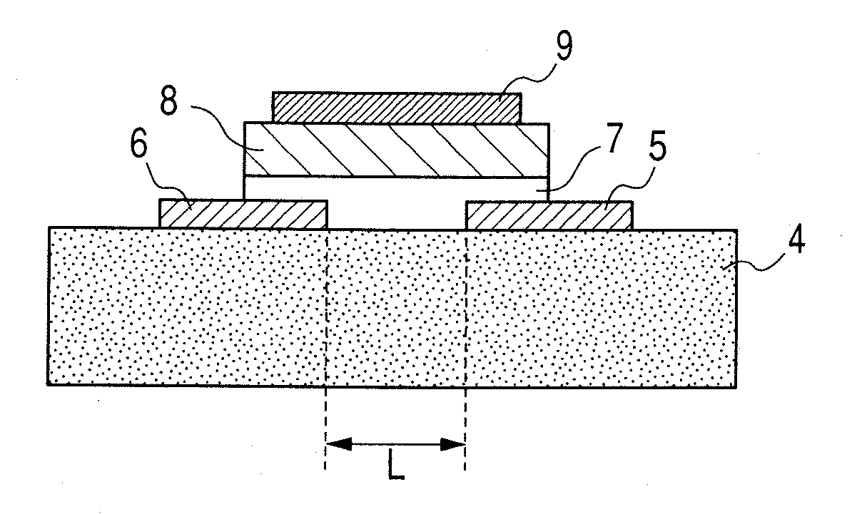
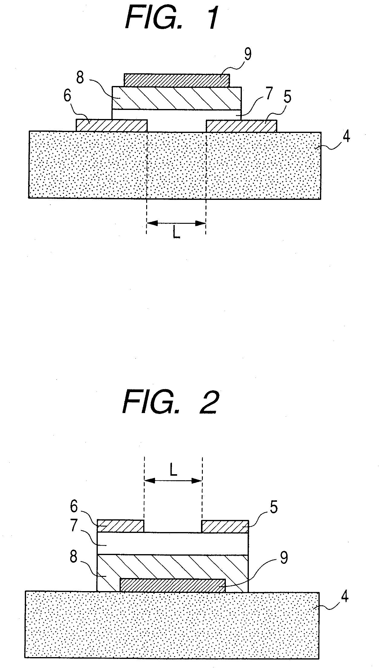
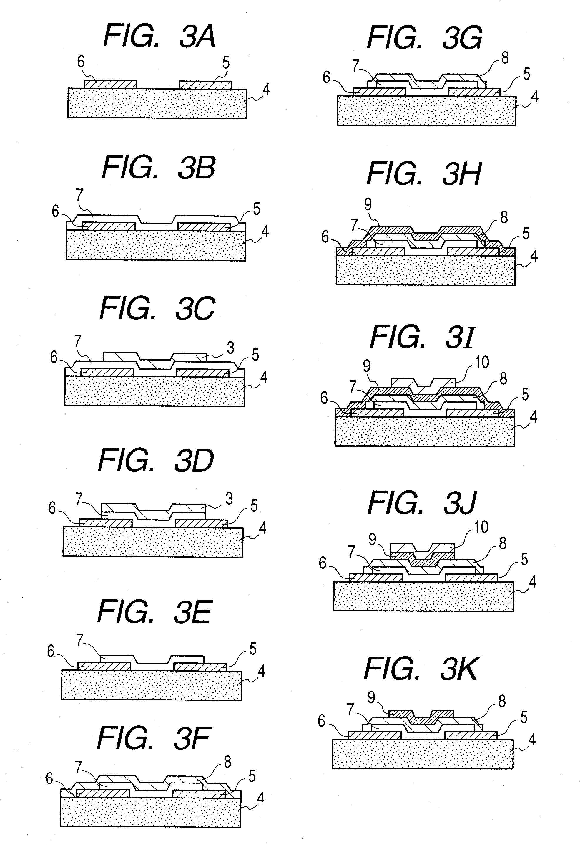
[0093]FIGS. 7A and 7B are a diagrammatic sectional view to illustrate a selective-etching method according to Example 2 of the present invention. In FIGS. 7A and 7B, reference numeral 1 denotes a material layer having a relatively low etch rate; and 2, a material layer having a relatively high etch rate. Reference numeral 3 denotes a resist layer which serves as an etching mask. Where the material layers 1 and 2 each have a low etching selectivity, the excess etch depth Δd of the material layer 1 becomes close to the undercut level Δw of the material layer 2. Where a thin-film transistor using such a structure is fabricated, the problem of scattering is raised in that the thin-film transistor has non-uniform characteristics.

[0094]An ITO layer is used as the material layer 1 and at least one selected from the group consisting of IZO, IGZO and IGO is used to form the material layer 2, so that the etching selectivity of the material layer 2 to the material layer 1 can ...


PUM

PropertyMeasurementUnit
thicknessaaaaaaaaaa
thicknessaaaaaaaaaa
thicknessaaaaaaaaaa

Abstract

An etching method is provided in which selective etching can be carried out for an amorphous oxide semiconductor film including at least one of gallium and zinc, and indium. In the etching method, the selective etching is performed using an alkaline etching solution. The alkaline etching solution contains especially ammonia in a specific concentration range.

Description

TECHNICAL FIELD[0001]This invention relates to an etching method, a pattern forming process, a thin-film transistor fabrication process and an etching solution (etchant) which are used in fabricating microelectronic component parts such as semiconductor devices, integrated circuits, and electrodes.BACKGROUND ART[0002]In recent years, as miniaturization, weight saving and electric power saving of electronic equipment are increasingly promoted, attention in the field of display is being focused on a semiconductor composed of an oxide IGZO including indium (In), gallium (Ga) and zinc (Zn). An IGZO amorphous oxide semiconductor film can be formed on a resin film at a low temperature, and hence, its application to light-weight portable electronic products in the future is being studied.[0003]Heretofore, films formed of the amorphous oxide including In, Ga and Zn have been subjected to patterning by a lift-off method (K. Nomura et. al., Nature, Vol. 432, 25, Nov. 2004, pp. 488-492). In th...

Claims


Application Information

Patent Timeline
Patent Type & Authority Applications(United States)
IPC IPC(8): H01L21/465C09K13/00
CPCH01L29/7869H01L29/66969H01L21/465H01L21/306H01L21/311
Inventor CHANG, CHIENLIU
Owner CANON KK
Why Eureka
Try Eureka