Iii-nitride semiconductor field effect transistor

Active Publication Date: 2010-02-18
MITSUBISHI ELECTRIC CORP
View PDF1 Cites 8 Cited by
  • Summary
  • Abstract
  • Description
  • Claims
  • Application Information

AI Technical Summary

Benefits of technology

[0010]According to the invention, since the lattice constant of the carrier travel layer is smaller than that of the undercoat layer, the carrier travel layer is subjected to tensile strain so as to apply a piezo effect, negative and positive charges are induced on a surface side of the carrier travel layer and a substrate side thereof, respectively, by the piezo effect. In addition, since the band gap of the carrier travel layer is smaller than that of the undercoat layer, two-dimensional electron gas is formed at an interface between the carrier travel layer and the undercoat layer, so that a reverse HEMT structure is made. As a result, ohmic electrodes contact the carrier travel layer having the lower Schottky barrier height, as compare

Problems solved by technology

However, the materials has the problems of current reduction due to voltage stress (current collapse), gate leakage current, h

Method used


Image

  • Iii-nitride semiconductor field effect transistor
  • Iii-nitride semiconductor field effect transistor
  • Iii-nitride semiconductor field effect transistor

Examples


first exemplary embodiment

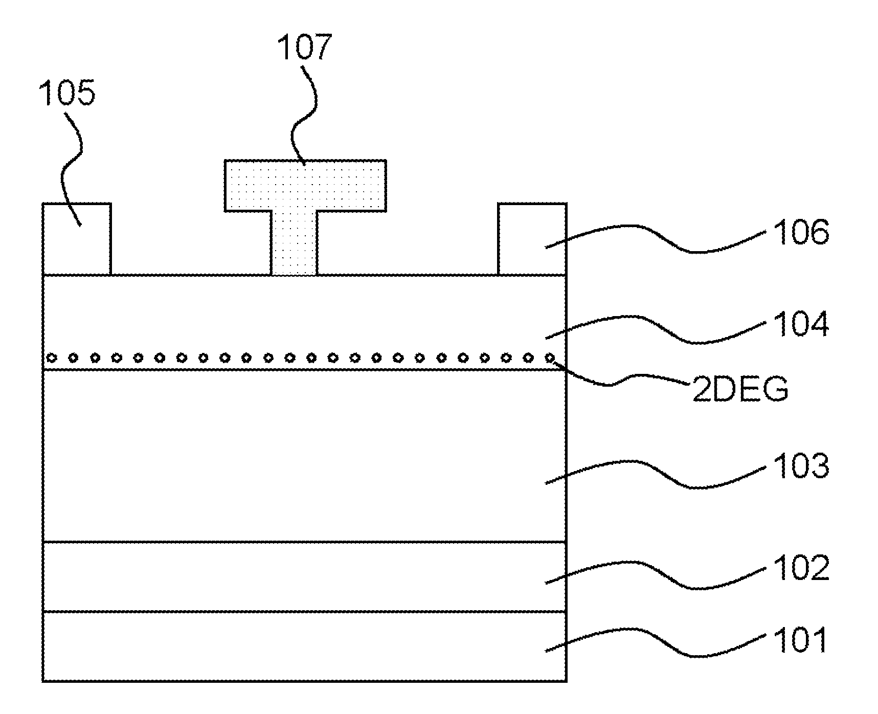
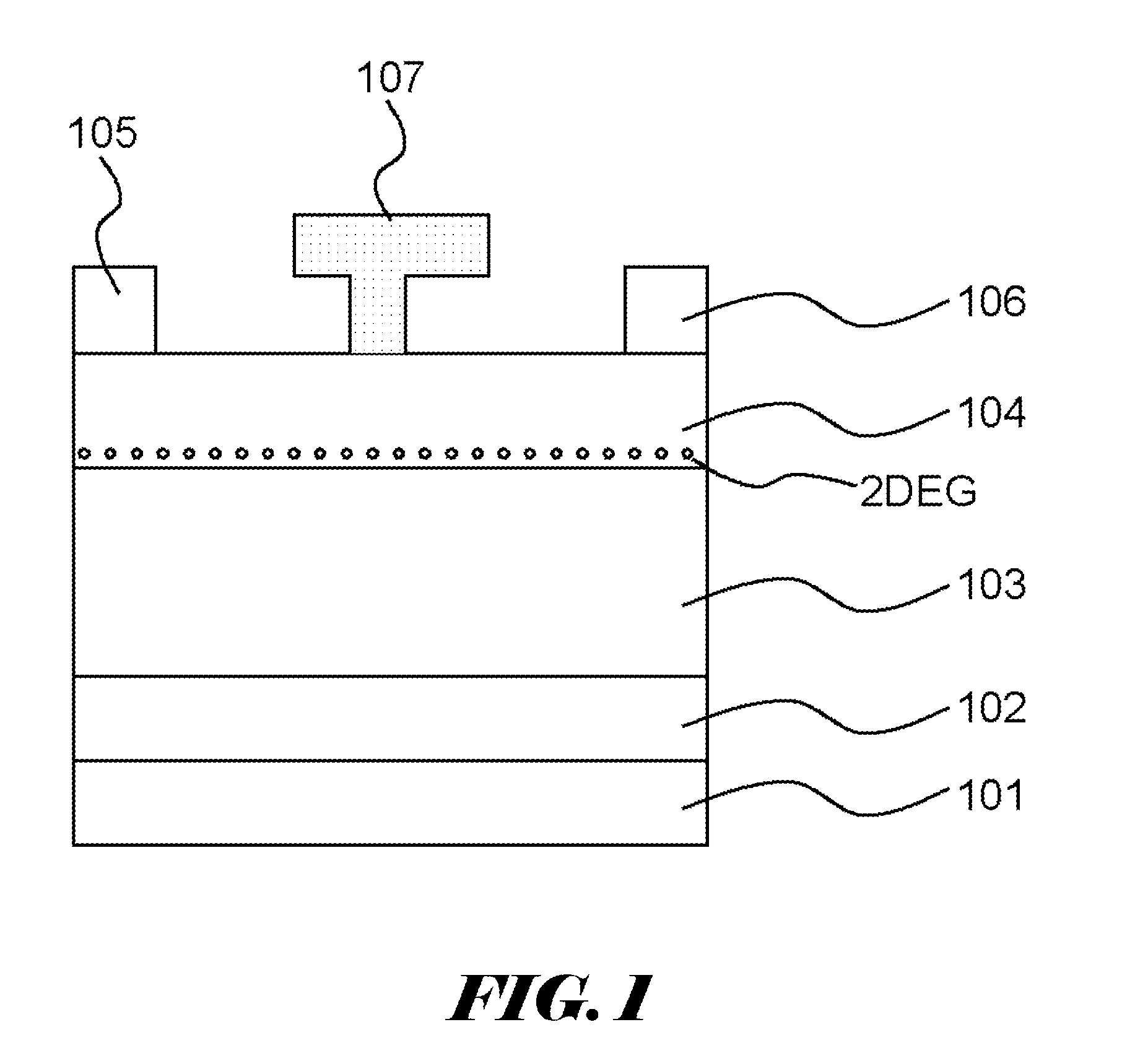
[0027]FIG. 1 is a sectional view showing a FET structure according to a first exemplary embodiment of the invention. The FET shown in FIG. 1 includes substrate 101 on which buffer layer 102 comprising a III-nitride semiconductor, undercoat layer 103 comprising a first III-nitride semiconductor and carrier travel layer 104 comprising a second III-nitride semiconductor are formed. Then, source electrode 105 and drain electrode 106 are formed. Further, gate electrode 107 is formed between source electrode 105 and drain electrode 106, so that a field effect transistor is thus manufactured.

[0028]As substrate 101, sapphire, silicon carbide, GaN, AlN and the like may be used.

[0029]As the III-nitride semiconductor constituting buffer layer 102, III-nitride semiconductor such as GaN, InN, AlN and a mixture of two or three species thereof may be used. Further, it may be possible that a nucleation layer comprising III-nitride semiconductor such as GaN, InN, AlN and a mixture of two or three sp...

second exemplary embodiment

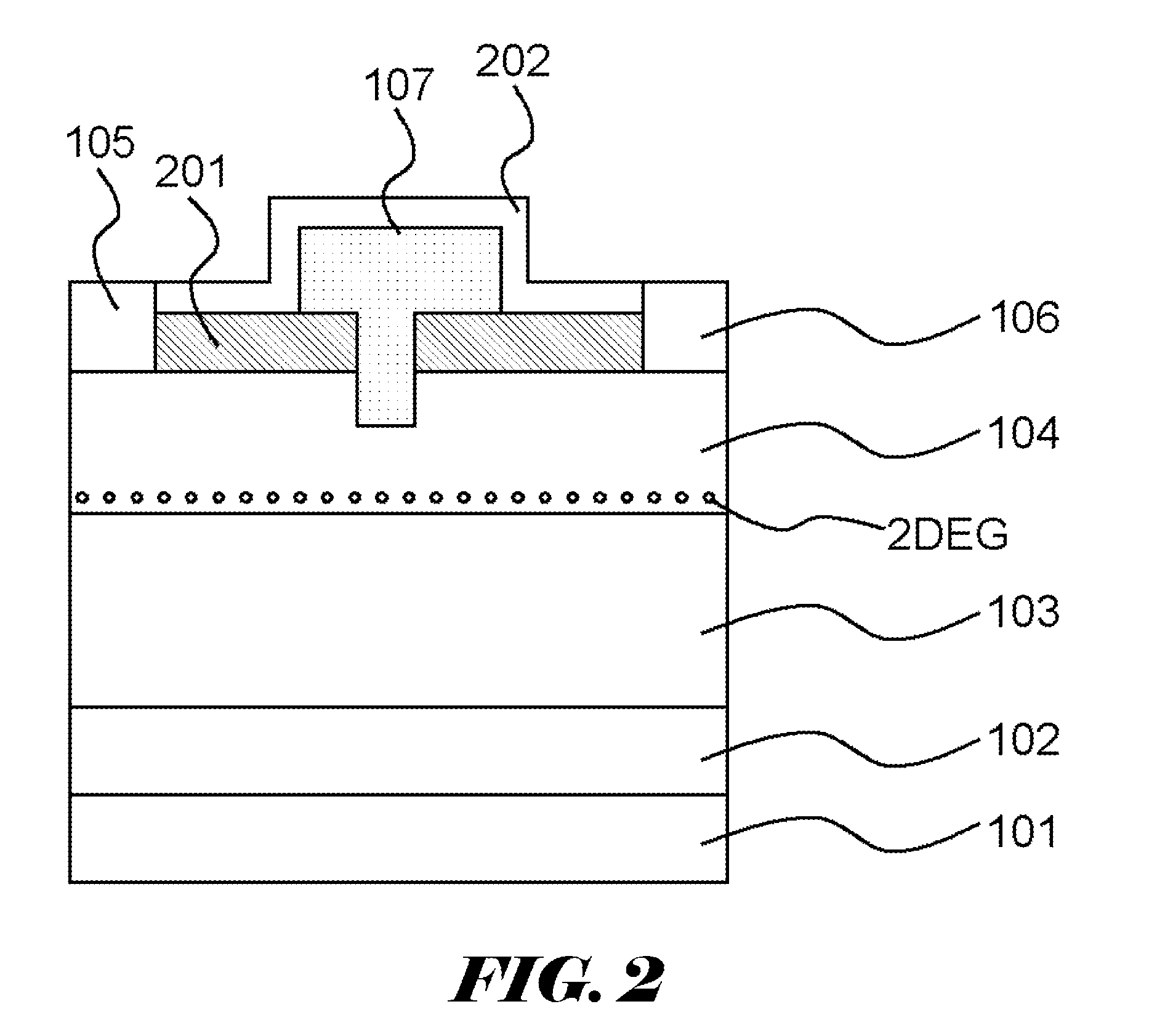
[0043]FIG. 2 is a sectional view showing a FET structure according to a second exemplary embodiment of the invention. In FIG. 2, the layers having the same functions as those shown in FIG. 1 are indicated with the same reference numerals and the description thereof will be omitted. Likewise the first exemplary embodiment, buffer layer 102, undercoat layer 103 and carrier travel layer 104 are formed on substrate 101. Then, source electrode 105 and drain electrode 106 are formed and first insulation film 201 is also formed. After that, a part of first insulation film 201 between source electrode 105 and drain electrode 106 is removed. Furthermore, a part of carrier travel layer 104 is removed by using insulation film 201 as a mask, so that a recess structure is formed. Subsequently, gate electrode 107 is formed in the part of the recess structure and on the remaining area of first insulation film 201 so that it is formed to be longer at a side facing the drain electrode side, as compa...

example 1

[0048]An example of the first exemplary embodiment of the invention will be described. The field effect transistor of the invention is manufactured by using c-plane ((0001) plane) silicon carbide (SiC) as substrate 101, AlN layer (film thickness: 200 nm) as buffer layer 102, InAlN layer (composition ratio of In: 0.2, film thickness: 2000 nm) as undercoat layer 103, GaN layer (film thickness: 30 nm) as carrier travel layer 104, Ti / Al (film thickness of Ti layer: 10 nm, thickness of Al layer: 200 nm) as source electrode 105 and drain electrode 106 and Ni / Au (film thickness of Ni layer: 10 nm, thickness of Au layer: 200 nm) as gate electrode 107, respectively.

[0049]To be more specific, buffer layer 102 was formed by the low temperatures (for example, 400-500° C.) metalorganic vapor phase epitaxy (MOVPE) method, undercoat layer 103 and carrier travel layer 104 were formed by the typical temperatures (for example, 800-1,100° C.) MOVPE method and source electrode 105 and drain electrode 1...


PUM


Abstract

Provided is a semiconductor device that can reduce the contact resistance, has a small current collapse, and can improve the pinch-off characteristic upon a high-frequency operation. A field effect transistor using a wurtzite (having (0001) as the main plane) type III-nitride semiconductor includes: a substrate (101); an undercoat layer (103) of a first III-nitride semiconductor; and a carrier travel layer (104) of a second III-nitride semiconductor. The undercoat layer (103) (101) and the carrier travel layer (104) is formed on the substrate in this order. The field effect transistor includes source/drain electrodes (105, 106) in ohmic contact, and a gate electrode (107) in Schottky contact directly or via another layer on the carrier travel layer (104). The undercoat layer (103) has an average lattice constant greater than that of the carrier travel layer (104) and a band gap greater than that of the carrier travel layer (104).

Description

TECHNICAL FIELD[0001]The present invention relates to a field effect transistor (FET) using a III-nitride semiconductor, and more particularly, to a high electron mobility transistor (HEMT).BACKGROUND ART[0002]Since a III-nitride semiconductor material having a large bandgap has characteristics of dielectric breakdown electric field having one higher order digit and high maximum electron velocity of two times or more, as compared to GaAs or Si, it is noted as a high power device material of microwave / milimetric wave bands. The HEMT using the material is expected as a high power transistor for next generation wireless communication. However, the materials has the problems of current reduction due to voltage stress (current collapse), gate leakage current, heat generation upon a high power operation and the like, which are causes of breakdown / output voltage decreases or instability. Hence, the most urgent necessity is to solve the above problems, thereby increasing the performance-rel...

Claims


Application Information

Patent Timeline
IPC IPC(8): H01L29/778
CPCH01L29/2003H01L29/7787H01L29/42316H01L29/7781
Inventor NAKAYAMA, TATSUOANDO, YUJIMIYAMOTO, HIRONOBUOKAMOTO, YASUHIROINOUE, TAKASHI
Owner MITSUBISHI ELECTRIC CORP
Why Eureka
Try Eureka