
Silicon wafer and method for manufacturing the same

Active Publication Date: 2010-02-25
SILTRONIC
View PDF11 Cites 14 Cited by
  • Summary
  • Abstract
  • Description
  • Claims
  • Application Information

AI Technical Summary

Benefits of technology

[0040]According to the present production process, the occurrence of both slips and warpages during a device production process can be considerably suppressed, and a high quality silicon wafer can be produced which does not have reduced strength despite having a DZ layer.

Problems solved by technology

If crystal defects are present on a surface where a circuit is formed, a circuit breakage is caused by the defects.
Meanwhile, a silicon wafer is required to include a proper amount of BMDs inside, since BMDs serve to getter metal impurities, which cause semiconductor device malfunction.
However, oxygen concentrations in DZ layers formed on the front and back faces of the silicon wafer by the above-mentioned high-temperature annealing process are extremely low because of the external diffusion of oxygen during heat treatment.
When the strength of a silicon wafer is reduced, the wafer could be damaged or broken during a production process.
In the process of JP 10-98047 previously discussed, reduction of silicon wafer strength was not considered, and in a silicon wafer produced thereby slip dislocation propagation cannot be avoided.
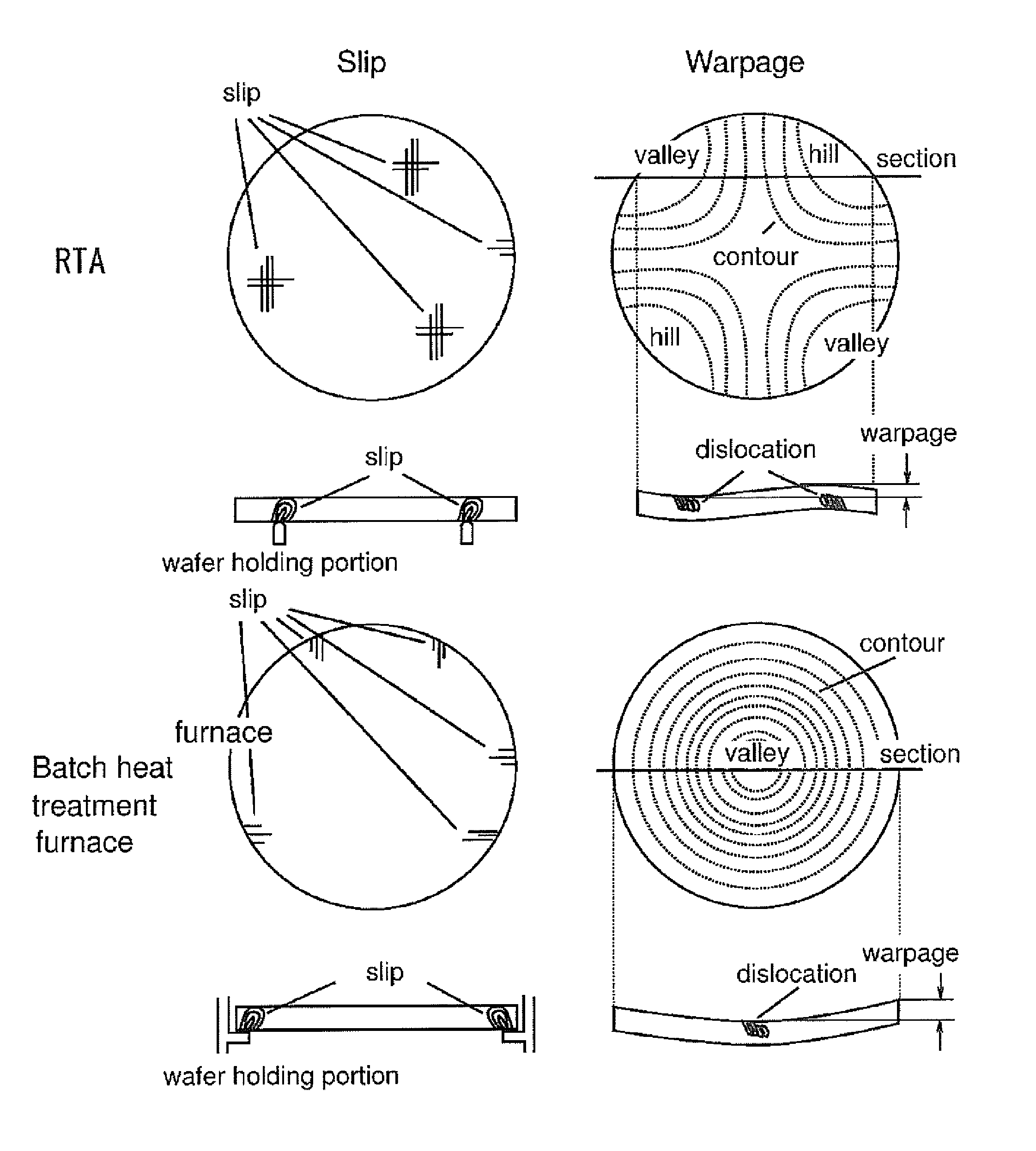
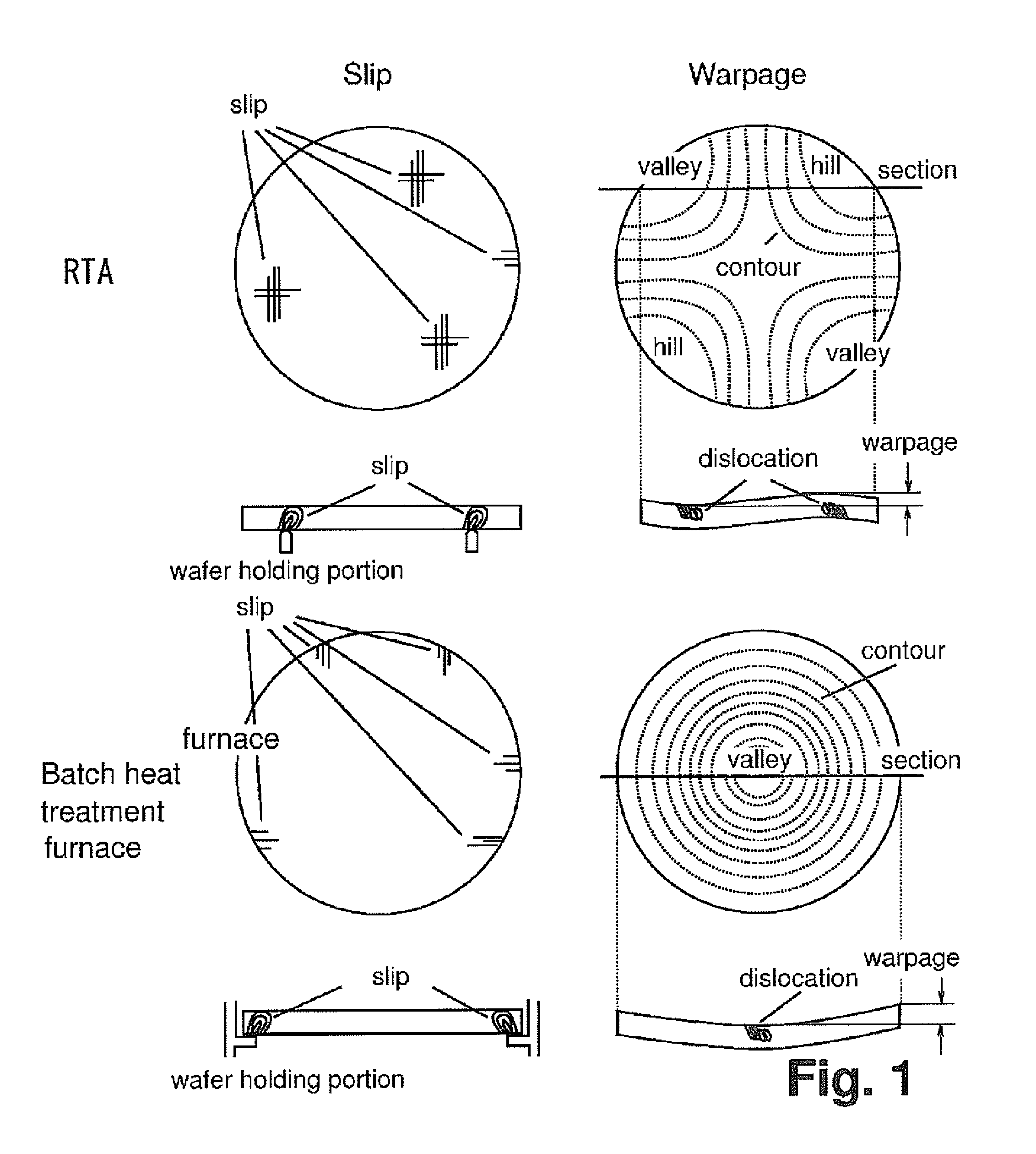
In recent years, because the diameter of silicon wafers has been increased and the degree of integration of semiconductor devices has also been increased, warpage of wafers has become problematic in addition to the problem of slip dislocations.
Warpage is a deformation caused by heat distortion during a heat treatment.
A large warpage prevents accurate exposure of a semiconductor device pattern on a wafer surface, causing the reduction in the yield of semiconductor devices.
The problem of warpages becomes serious when the wafer diameter is 200 mm or more.
This problem could not be avoided simply by requiring a high density of BMDs as above.

Method used


Image

  • Silicon wafer and method for manufacturing the same
  • Silicon wafer and method for manufacturing the same
  • Silicon wafer and method for manufacturing the same

Examples


examples

[0087]The present invention is illustrated by the examples in the following section, but it is not limited to those examples.

Process for Producing Annealed Wafer

[0088]Single crystal ingots were produced under various conditions (wafer diameter, conduction type, oxygen-, nitrogen- and carbon concentrations). Wafers were sawn from the constant diameter portion of the obtained single crystal ingots using a wire saw and subjected to a mirror treatment to form substrates with a thickness of 725 to 750 μm. From these substrates, annealed wafers were produced by the following processes (1) and (2):

(1) Heat Treatment 1

[0089]The obtained substrates were inserted into a batch vertical heat treatment furnace, and subjected to a first heat treatment (A, B and C) and the second heat treatment (D) in an argon atmosphere in the same furnace. The diffusion lengths of the interstitial oxygen in the second heat treatment were obtained by integrating the formula (i) provided previously on the basis of...


PUM


Abstract

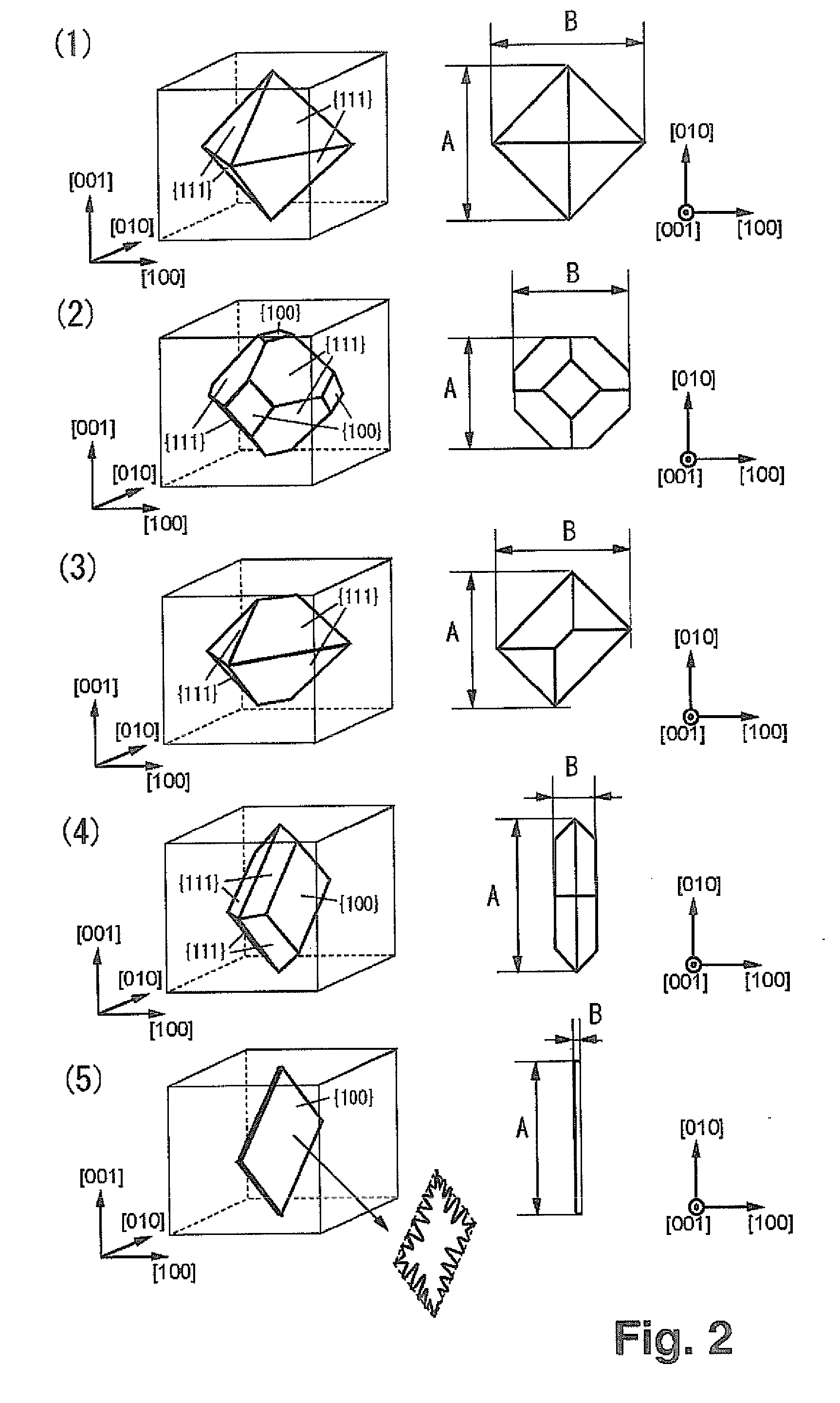
Silicon wafers wherein slip dislocations and warpages during device production are suppressed, contain BMDs with an octahedral shape, and of BMDs at a depth greater than 50 μm from the surface of the wafer, the density of BMDs with diagonal size of 10 nm to 50 nm is ≧1×10¹² / cm3, and the density of BSFs is ≦1×10⁸ / cm3. The present silicon wafers preferably have an interstitial oxygen concentration of 4×10¹⁷ atoms / cm3 to 6×10¹⁷ atoms / cm3, and a density of BMDs with diagonal size of ≧200 nm of not more than 1×10⁷ / cm3.

Description

CROSS-REFERENCE TO RELATED APPLICATIONS[0001]This application is a continuation-in-part of PCT / JP2008 / 058359 filed May 1, 2008 which claims priority to JP Priority Applications JP 2007-121773 filed May 2, 2007, and JP 2007-338842 filed Dec. 28, 2007, all of which are herein incorporated by reference.BACKGROUND OF THE INVENTION[0002]1. Field of the Invention[0003]The present invention relates to the technical field of semiconductor wafer production, particularly to a silicon wafer wherein the occurrence of both slip dislocations and warpages during a device production process can be suppressed, and to a process for producing the same.[0004]2. Description of the Related Art[0005]A silicon wafer used as a substrate for semiconductor devices is produced by slicing a silicon single crystal ingot and subjecting the sliced wafers to heat treatment, mirror finishing, and the like. One process for producing silicon single crystal ingots is the Czochralski method (CZ method). The CZ method ac...

Claims


Application Information

Patent Timeline
IPC IPC(8): B32B3/00H01L21/322
CPCC30B29/06Y10T428/26H01L21/3225C30B33/02H01L21/322
Inventor NAKAI, KATSUHIKOFUKUDA, MASAYUKI
Owner SILTRONIC
Learn More