Semiconductor memory device

a memory device and semiconductor technology, applied in semiconductor devices, digital storage, instruments, etc., can solve the problems of high cost, large area occupied by the device, and volatile memories that cannot hold data without power supply, and achieve the effect of low cost and high performan

Inactive Publication Date: 2010-04-01
SHARP KK
View PDF11 Cites 23 Cited by
  • Summary
  • Abstract
  • Description
  • Claims
  • Application Information

AI Technical Summary

Benefits of technology

[0065]Although the semiconductor memory device according to the present invention has both the memory function of a volatile memory and that of a nonvolatile memory, it is possible that part of the region of the memory cells arranged in a matrix is used only as a nonvolatile memory region and the volatile memory function is not used. At this time, the conditions for operations such as optimal voltage to be applied in the above described set operation mode and reset operation mode are stored in the nonvolatile memory region, so that the conditions for operation stored in the nonvolatile memory region are read out in each operation mode, and thus, the states of th

Problems solved by technology

Memory data in SRAMs and DRAMs can be read out and written at a high speed and at random, and thus, they are memories that can be very easily handled, but they are volatile memories that cannot hold data without a power supply.
SRAMs have better performance than DRAMs in the speed of operation and the holding of data as volatile memories, but the area occupied by the device is greater and the cost is higher, and therefore, the majority of the market is occupied by DRAMs, of which the cost is lower.
In recent years, however, the limits of miniaturization have been pointed out mainly due to the difficulty in the scaling down of the capacitor, and under such circumstances, research has been performed as in Documents 1 to 4 cited below on one-transistor type DRAMs where a majority carrier is accumulated in the channel body of the transistor so that the memory is held.
Flash memories are non-volatile memories which hold memory even when the power supply is turned off, but there is a limitation in the method for writing and reading out as well as the rate of writing and the number of times of writing, and thus, flash memories are not easy to use as compared to DRAMs and SRAMs.
A non-volatile memory where random writing and random reading out are possible can be implemented theoretically by FeRAMs, PCRAMs, RRAMs and MRAMs, but their writing performance is inferior to that of the conventional DRAMs.
However, the number of times of possible writing is approximately 109 at the most, though it has been increasing year after year, and thus, no RRAMs can be used as a DRAM where writing is always possible.
Though the number of times of possible writing is greater in FeRAMs than in PCRAMs or RRAMs, it is still difficult for FeRAMs to be substituted for DRAMs due t

Method used


Image

  • Semiconductor memory device
  • Semiconductor memory device
  • Semiconductor memory device

Examples


first embodiment

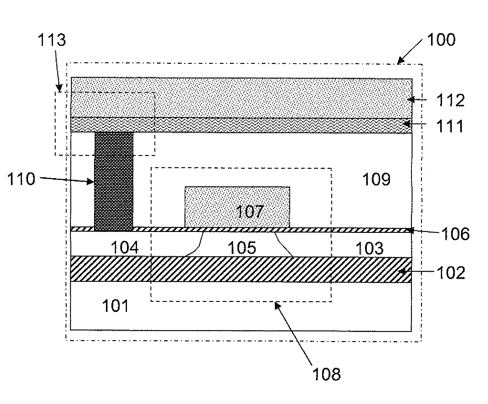
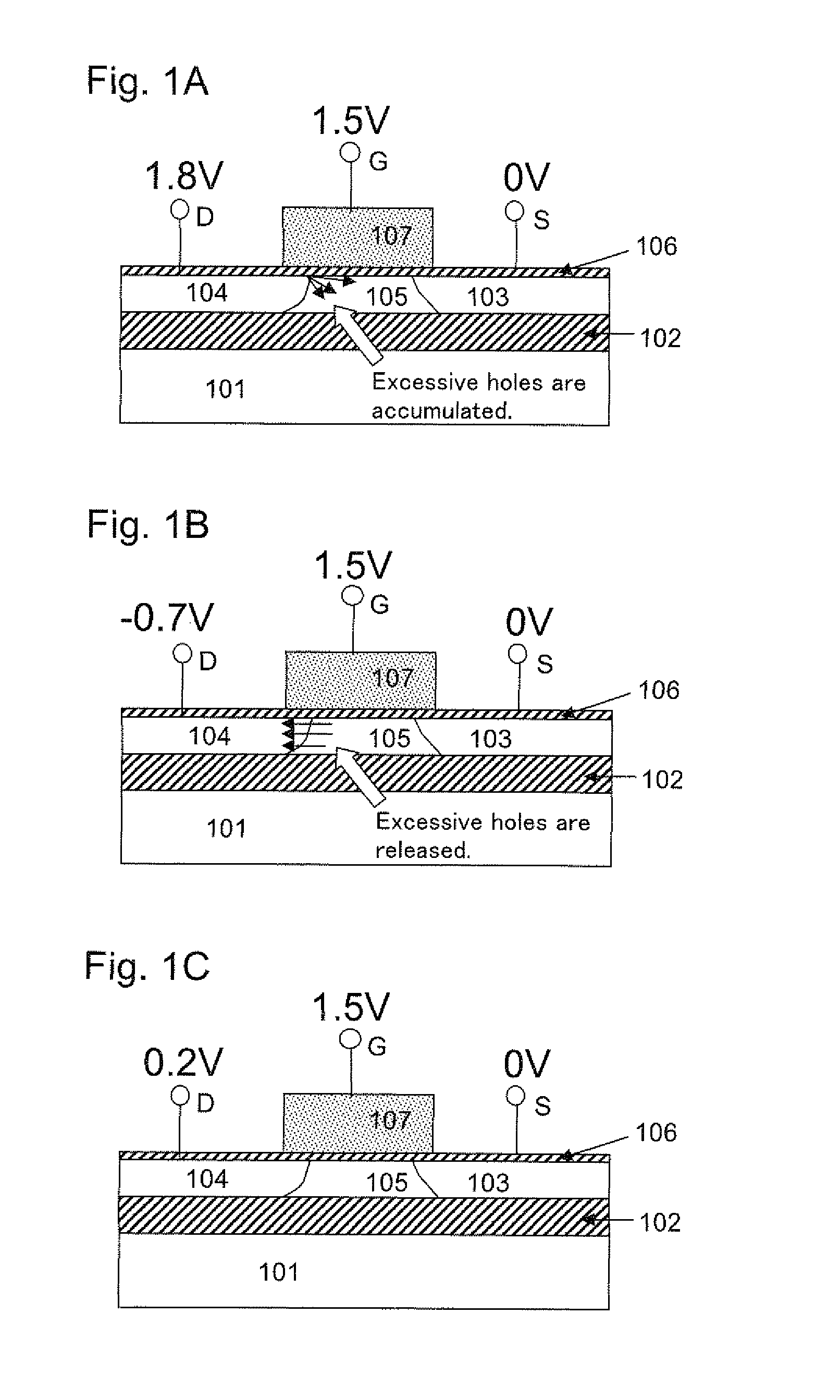
[0089]FIG. 5 is a cross-sectional diagram showing the structure of a memory cell 100 in the semiconductor memory device according to the first embodiment of the present invention. An insulating film (silicon oxide film) 102 is formed on a silicon substrate 101, and an n type source region 103, an n type drain region 104 and a p type channel body region 105 of a MISFET 108 are formed in the semiconductor layer (SOI substrate), which is electrically isolated from the semiconductor substrate 101 by means of the insulating film 102. A gate electrode 107 is formed above the channel body region 105 with a second insulating film 106 in between. An interlayer insulating film 109 is formed over the MISFET 108, and a contact hole is created in the interlayer insulating film 109 for contact on the upper surface of the drain region 104, and the contact hole is filled in with a contact plug 110. The contact plug 110 is formed by combining a barrier metal of Ti / TiN and W, which is the same as gen...

second embodiment

[0109]The semiconductor memory device according to the present invention operates in accordance with the above described operation method, and thus, a nonvolatile semiconductor memory device where random write and readout are possible an unlimited number of times can be provided. The system configuration is shown in the following.

[0110]As shown in FIG. 18, the semiconductor memory device system according to the present invention is formed of a memory cell array 201 which is formed in accordance with the first embodiment of the present invention, a word decoder 202 which is connected to the word lines of the memory cell array 201 and driven by selecting the memory cells within the memory cell array 201 in the row direction, a sense amplifier 203 which is connected to the bit lines of the memory cell array 201, a column decoder 204 for selecting the memory cells within the memory cell array 201 in the column direction, and an interface control circuit 205 for controlling the voltage a...

third embodiment

[0112]FIG. 19 shows the structure of the semiconductor memory device (memory cell array) according to the third embodiment of the present invention, and FIGS. 20A and 20B show the structure in a cross section. FIGS. 20A and 20B are cross-sectional diagrams along A-A′ and B-B′, respectively, in FIG. 19. FIG. 21 shows an equivalent circuit of the structure in FIGS. 19, 20A and 20B. The third embodiment is different from the first embodiment in that the MISFETs having a channel body, which is electrically isolated from the semiconductor substrate, are provided as vertical transistors with the channel body region covered with an insulating film.

[0113]Vertical transistors in column form are formed in the direction of the depth such that n type source regions 302, p type channel body regions 303 and n type drain regions 304 are formed on top of a p type semiconductor substrate 301 in this order. Herein, the source regions are connected in the row direction (A-A′ direction), so that source...


PUM


Abstract

An inexpensive nonvolatile memory having high performance which makes random write and readout possible an unlimited number of times is provided. A unit memory cell is formed of a MISFET having a channel body that is electrically isolated from a semiconductor substrate and a resistance change element having a two-terminal structure with one end electrically connected to a drain of the MISFET. The MISFET functions as a volatile memory element, and the resistance change element functions as a nonvolatile memory element, so that information stored in the MISFET is copied to the resistance change element before the power is turned OFF and information stored in the resistance change element is transferred to the MISFET when the power is turned ON, and thus, the MISFET is used as a volatile memory which makes random write and readout possible.

Description

CROSS REFERENCE TO RELATED APPLICATION[0001]This Nonprovisional application claims priority under 35 U.S.C. §119(a) on Patent Application No. 2008-248180 filed in Japan on 26 Sep. 2008 the entire contents of which are hereby incorporated by reference.BACKGROUND OF THE INVENTION[0002]1. Field of the Invention[0003]The present invention relates to a semiconductor memory device.[0004]2. Description of the Related Art[0005]Semiconductor memory devices are currently indispensable key devices for electronic devices. Semiconductor memory devices are mainly categorized into volatile memories represented by SRAMs and DRAMs and non-volatile memories represented by flash memories. Memory data in SRAMs and DRAMs can be read out and written at a high speed and at random, and thus, they are memories that can be very easily handled, but they are volatile memories that cannot hold data without a power supply.[0006]SRAMs have better performance than DRAMs in the speed of operation and the holding of...

Claims


Application Information

Patent Timeline
IPC IPC(8): G11C11/00G11C7/00H01L47/00
CPCG11C11/005G11C13/0004G11C13/0007G11C13/0033G11C2211/4016G11C2213/31H01L27/2472H01L45/06H01L45/085H01L45/1233H01L45/146H01L27/2436H01L27/2454H01L45/04G11C13/0011G11C14/00G11C14/0045H10B63/30H10B63/34H10B63/82H10N70/20H10N70/245H10N70/231H10N70/826H10N70/8833
Inventor AWAYA, NOBUYOSHINAKANO, TAKASHI
Owner SHARP KK
Why Eureka
Try Eureka