Electroluminescent devices including organic eil layer

a technology of electroluminescent devices and electron injection layers, which is applied in the direction of thermoelectric device junction materials, semiconductor devices, electrical apparatus, etc., can solve the problems of large efficiency loss, performance limitations, and many desirable applications, and achieve improved electroluminescent features, reduced operational voltage, and high luminous efficiency

Active Publication Date: 2010-04-08
GLOBAL OLED TECH
View PDF100 Cites 39 Cited by
  • Summary
  • Abstract
  • Description
  • Claims
  • Application Information

AI Technical Summary

Benefits of technology

[0014]The device of the invention exhibit provides improved electroluminesce

Problems solved by technology

While organic electroluminescent (EL) devices have been known for over two decades, their performance limitations have represented a barrier to many desirable applications.
However, it is generally

Method used


Image

  • Electroluminescent devices including organic eil layer
  • Electroluminescent devices including organic eil layer
  • Electroluminescent devices including organic eil layer

Examples


examples

[0321]The invention and its advantages can be better appreciated by the following examples.

Device Examples 1-1 Through 1-6

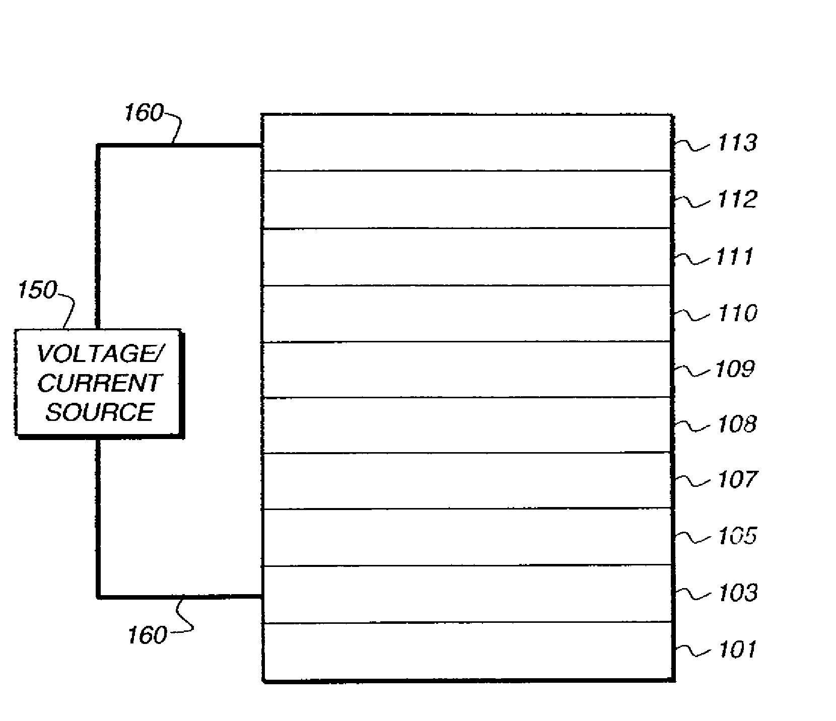
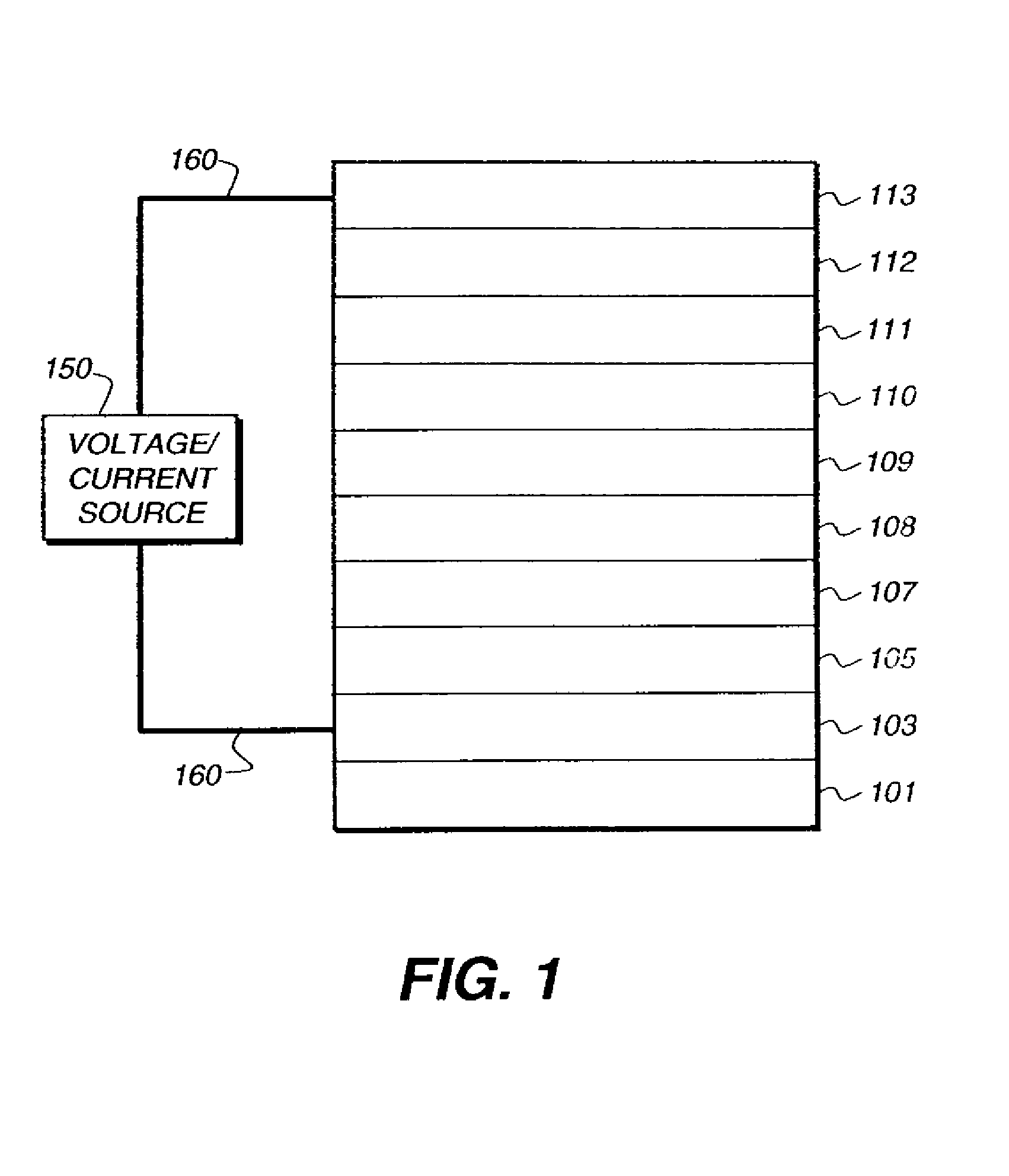
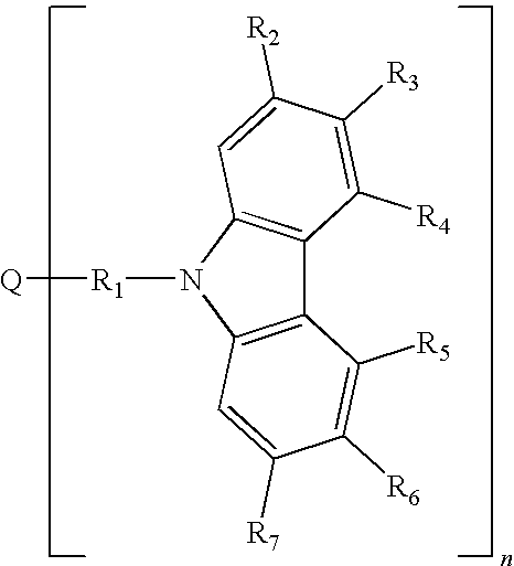
[0322]An EL device (Device 1-1) was constructed in the following manner:[0323]1. A glass substrate, coated with an approximately 25 nm layer of indium-tin oxide (ITO) as the anode, was sequentially ultrasonicated in a commercial detergent, rinsed in deionized water, degreased in toluene vapor and exposed to an oxygen plasma for about 1 minute.[0324]2. Over the ITO a 1 nm fluorocarbon (CFx) hole injecting layer (HIL) was deposited by plasma-assisted deposition of CHF3 as described in U.S. Pat. No. 6,208,075.[0325]3. Next, a hole transporting layer (HTL) of N,N′-di-1-naphthyl-N,N′-diphenyl-4,4′-diaminobiphenyl (NPB) was vacuum deposited to a thickness of 75 nm.[0326]4. An exciton / electron blocking layer (EBL) of 4,4′,4″-tris(carbazolyl)-triphenylamine (TCTA) was vacuum deposited to a thickness of 10 nm.[0327]5. A 35 nm light emitting layer (LEL) consisting of a mix...

example series 15-1 and 15-2

Device Example Series 15-1 and 15-2

[0426]Orange-emitting phosphorescent EL devices 15-1 to 15-2 were constructed using vapor deposition techniques in the following sequence:[0427]1. A glass substrate coated with a 57 nm layer of indium-tin oxide (ITO) as the anode was sequentially ultrasonicated in a commercial detergent, rinsed in deionized water, dried, and heated at 130° C. about 12 hours.[0428]2. A 10 nm thick hole-injection layer (HIL) of a hole-injecting material DQHC was then deposited.[0429]3. A 70 nm hole transport layer (HTL1) of NPB was then deposited onto HIL.[0430]4. A 40 nm light emitting layer comprising consisting of a mixture of INV-1 as the electron transporting co-host, PHF-19 as the hole transporting (HT) co-host, PD-19 as a yellow phosphorescent emitter and PD-20 as a red phosphorescent emitter was then vacuum deposited onto the HTL. The PHF-19 comprises 15 wt. % of the total of the co-host materials in the LEL, the PD-19 comprises 18 wt. % and the PD-20 compris...

example series 16-1 and 16-2

Device Example Series 16-1 and 16-2

[0437]White tandem EL devices 16-1 to 16-2 were constructed using vapor deposition techniques in the following sequence:[0438]1. A glass substrate coated with a 57 nm layer of indium-tin oxide (ITO) as the anode was sequentially ultrasonicated in a commercial detergent, rinsed in deionized water, dried and heated at 130° C. about 12 hours.[0439]2. A 10 nm thick hole-injection layer (HIL) of a hole-injecting material DQHC was then deposited.[0440]3. A 150 nm hole transport layer (HTL1) of NPB was then deposited onto HIL.[0441]4. A 30 nm thick blue light-emitting layer (BLEL) comprising the host material 9-(1-naphthyl)-10-(2-naphthyl)anthracene (NNA) and 5.0% of blue-emitting fluorescent material BD-1 was then deposited.

[0442]5. A 10 nm thick hole blocking layer (HBL1) of Inv-24 was then deposited.[0443]6. A 30 nm thick n-doped electron transporting layer (ETL1) consisting of a mixture of 49% LiQ, 49% Bphen, and 1% metal Li was then deposited.[0444]7...


PUM


Abstract

An OLED device comprises a cathode, an anode, and has therebetween a light emitting layer (LEL) comprising a phosphorescent emitting compound disposed in a host comprising a mixture of at least one electron transporting co-host which is a benzophenone derivative with a spiro substituent and at least one hole transporting co-host which is a triphenylamine which contains one trivalent nitrogen atom that is bonded only to carbon atoms, at least one of which is a member of an aromatic ring, wherein there is present an electron transporting layer contiguous to the LEL (HBL?) on the cathode side comprising an anthracene or a fluoranthene and wherein there is present an election injecting layer comprising a phenanthroline or a lithium quinolate contiguous to the cathode.

Description

CROSS-REFERENCE TO RELATED APPLICATION[0001]This application is a continuation-in-part of U.S. application Ser. No. 11 / 412,544 filed Apr. 27, 2006.FIELD OF INVENTION[0002]This invention relates to organic electroluminescent (EL) devices. More specifically, this invention relates to phosphorescent devices including an electron injection layer.BACKGROUND OF THE INVENTION[0003]While organic electroluminescent (EL) devices have been known for over two decades, their performance limitations have represented a barrier to many desirable applications. In simplest form, an organic EL device is comprised of an anode for hole injection, a cathode for electron injection, and an organic medium sandwiched between these electrodes to support charge recombination that yields emission of light. These devices are also commonly referred to as organic light emitting diodes, or OLEDs. Representative of earlier organic EL devices are Gurnee et al. U.S. Pat. No. 3,172,862, issued Mar. 9, 1965; Gurnee U.S....

Claims


Application Information

Patent Timeline
IPC IPC(8): H01L51/54
CPCH01L51/0058H01L51/0059H01L51/006H01L51/0067H01L51/0069H01L51/5096H01L51/0081H01L51/0085H01L51/5016H01L51/5048H01L51/5092H01L51/0072H10K85/631H10K85/626H10K85/656H10K85/633H10K85/654H10K85/6572H10K85/324H10K85/342H10K50/11H10K2101/10H10K50/14H10K50/171H10K50/18H10K85/30H10K85/60H10K85/326H10K85/622H10K50/16H10K85/615
Inventor KONDAKOVA, MARINA E.KONDAKOV, DENIS Y.BROWN, CHRISTOPHER T.HATWAR, TUKARAM K.SPINDLER, JEFFREY P.
Owner GLOBAL OLED TECH
Why Eureka
Try Eureka