Semiconductor device and manufacturing method thereof

a semiconductor layer and semiconductor technology, applied in the direction of semiconductor devices, basic electric elements, electrical appliances, etc., can solve the problems of aluminum atoms being likely to be diffused, the electrical characteristics and reliability of thin film transistors are impaired, etc., and achieve the effect of suppressing the diffusion of aluminum atoms to the oxide semiconductor layer

Active Publication Date: 2010-04-15
SEMICON ENERGY LAB CO LTD
View PDF100 Cites 103 Cited by
  • Summary
  • Abstract
  • Description
  • Claims
  • Application Information

AI Technical Summary

Benefits of technology

[0022]According to an embodiment of the present invention, the second conductive layers formed using a high-melting-point metal material or the barrier layers including aluminum oxide as a main component are formed between the oxide semiconductor layer including indium, gallium, and zinc and the first conductive layers including aluminum as a main component; accordingly, aluminum atoms can be prevented from being diffused into the oxide semiconductor layer. In particular, even when the oxide semico

Problems solved by technology

However, electric characteristics and reliability of the thin film transistor are, in some cases, impaired by diffusion of an impurity element into a channel region.
Further, the structure in which the first conductive layers including aluminum as a main component sandw

Method used


Image

  • Semiconductor device and manufacturing method thereof
  • Semiconductor device and manufacturing method thereof
  • Semiconductor device and manufacturing method thereof

Examples


embodiment 1

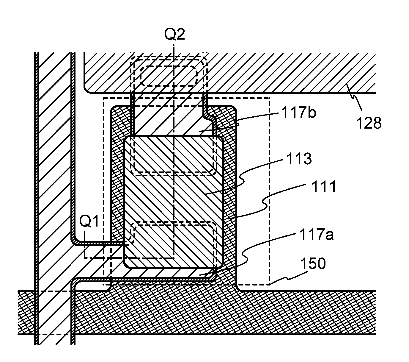
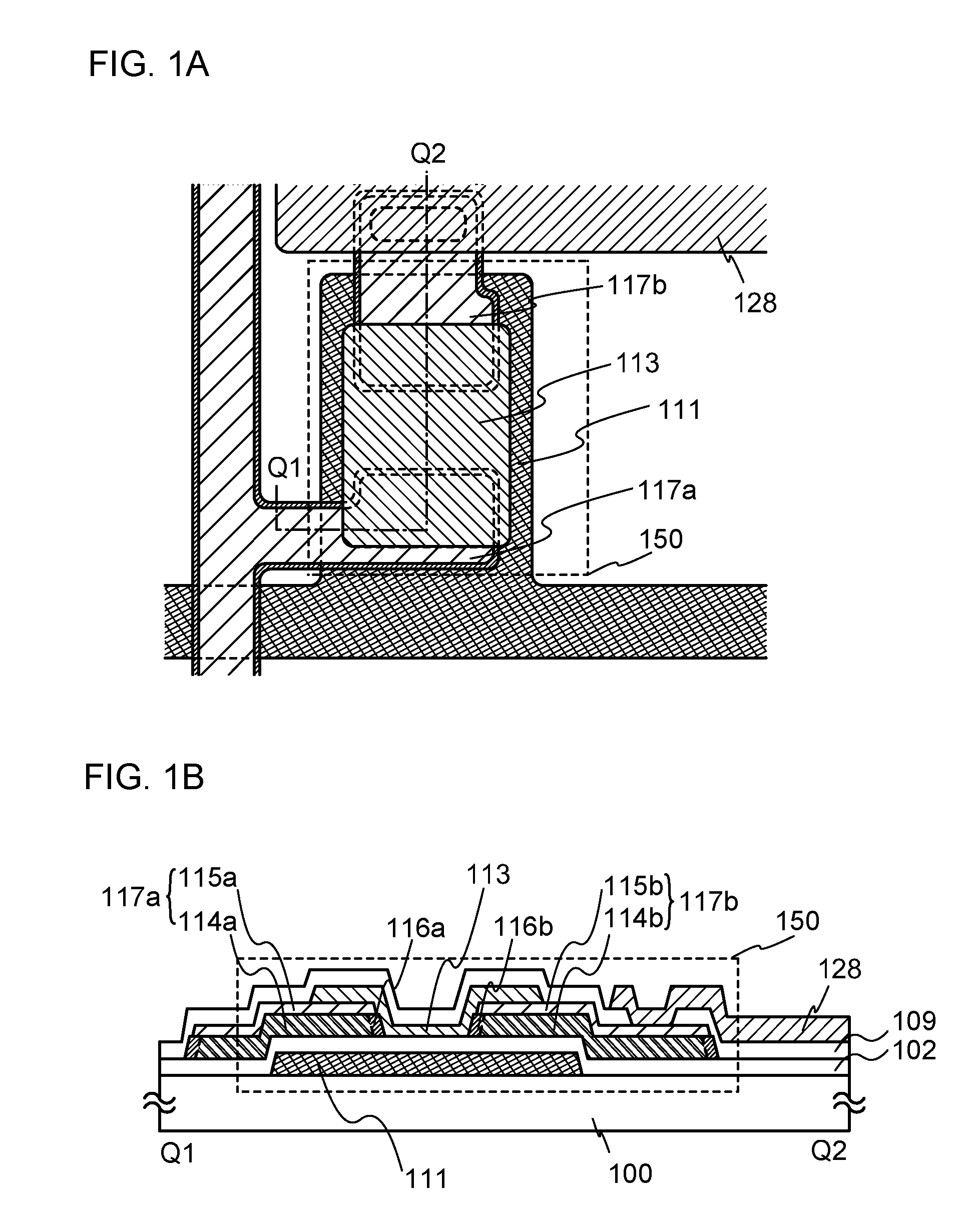
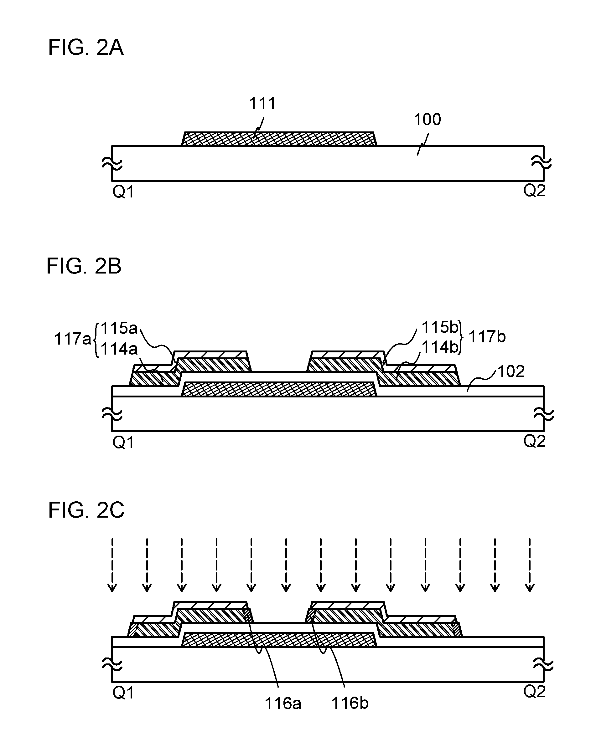
[0048]In Embodiment 1, a thin film transistor and a manufacturing process thereof will be described with reference to FIGS. 1A and 1B, FIGS. 2A to 2C, and FIGS. 3A to 3C.

[0049]FIGS. 1A and 1B illustrate a thin film transistor of this embodiment. FIG. 1A is a plan view and FIG. 1B is a cross-sectional view taken along line Q1-Q2 in FIG. 1A. In a thin film transistor 150 illustrated in FIGS. 1A and 1B, a gate electrode layer 111 is formed over a substrate 100, and a gate insulating film 102 is formed over the gate electrode layer 111. Source or drain electrode layers (117a, 117b) are formed over the gate insulating film 102 by stacking second conductive layers (115a, 115b) which are formed using a high-melting-point metal material over first conductive layers (114a, 114b) including aluminum as a main component so that end portions of the source or drain electrode layers (117a, 117b) overlap the gate electrode layer 111. An oxide semiconductor layer 113 is formed so as to overlap the g...

embodiment 2

[0093]In Embodiment 2, a thin film transistor and a manufacturing method thereof, which are different from those in Embodiment 1, will be described with reference to FIGS. 4A and 4B, FIGS. 5A to 5C, and FIGS. 6A to 6C.

[0094]FIGS. 4A and 4B illustrate an embodiment different from that of Embodiment 1. FIG. 4A is a plan view and FIG. 4B is a cross-sectional view taken along line Q1-Q2 in FIG. 4A.

[0095]In a thin film transistor 151 illustrated in FIGS. 4A and 4B, source or drain electrode layers (117a, 117b) are formed over a substrate 100. In the source or drain electrode layers (117a, 117b), second conductive layers (115a, 115b) which are formed using a high-melting-point metal material are stacked over first conductive layers (114a, 114b) including aluminum as a main component. An oxide semiconductor layer 113 is formed to be in contact with the second conductive layers (115a, 115b) which are formed using a high-melting-point metal material in the source or drain electrode layers an...

embodiment 3

[0116]In Embodiment 3, an example of electronic paper will be described as a display device which is an example of a semiconductor device according to an embodiment of the present invention.

[0117]FIG. 7 illustrates active-matrix electronic paper as an example of a display device to which an embodiment of the present invention is applied. A thin film transistor 581 used in the display device can be manufactured in a manner similar to that of Embodiment 1 or 2 and has high reliability with suppression in diffusion of aluminum atoms to an oxide semiconductor layer.

[0118]The electronic paper in FIG. 7 is an example of a display device using a twisting ball display system. The twisting ball display system refers to a method in which spherical particles each colored in black and white are used for a display element and arranged between a first electrode layer and a second electrode layer which are electrode layers, and a potential difference is generated between the first electrode layer ...


PUM


Abstract

Electric characteristics and reliability of a thin film transistor are impaired by diffusion of an impurity element into a channel region. The present invention provides a thin film transistor in which aluminum atoms are unlikely to be diffused to an oxide semiconductor layer. A thin film transistor including an oxide semiconductor layer including indium, gallium, and zinc includes source or drain electrode layers in which first conductive layers including aluminum as a main component and second conductive layers including a high-melting-point metal material are stacked. An oxide semiconductor layer 113 is in contact with the second conductive layers and barrier layers including aluminum oxide as a main component, whereby diffusion of aluminum atoms to the oxide semiconductor layer is suppressed.

Description

BACKGROUND OF THE INVENTION[0001]1. Field of the Invention[0002]An embodiment of the present invention relates to a semiconductor device having a circuit including a thin film transistor (hereinafter referred to as a TFT) in which an oxide semiconductor film is used for a channel formation region, and a manufacturing method thereof. For example, the present invention relates to an electronic appliance on which an electro-optical device typified by a liquid crystal display panel or a light-emitting display device having an organic light-emitting element is mounted as a component. It is to be noted that the semiconductor devices in this specification indicate all the devices which can operate by using semiconductor characteristics, and an electro-optical device, a semiconductor circuit, and an electronic appliance are all included in the semiconductor devices.[0003]2. Description of the Related Art[0004]Recently, active-matrix display devices (such as liquid crystal display devices, l...

Claims


Application Information

Patent Timeline
IPC IPC(8): H01L29/24H01L21/34
CPCH01L27/1225H01L29/7869H01L29/78606H01L29/45H01L29/66742
Inventor AKIMOTO, KENGO
Owner SEMICON ENERGY LAB CO LTD
Why Eureka
Try Eureka