Display element

a display element and display technology, applied in non-linear optics, instruments, optics, etc., can solve the problems of certain viewer-friendly, light-emitting display, eye fatigue, etc., and achieve the effect of minimal variation in reflectance and enhanced display contras

Inactive Publication Date: 2010-04-22
KONICA MINOLTA INC
View PDF5 Cites 14 Cited by
  • Summary
  • Abstract
  • Description
  • Claims
  • Application Information

AI Technical Summary

Benefits of technology

[0026]According to the present invention, there was able to be provided a display element with a simple member structure being drivable at low voltage which is a display element exhibiting enhanced display contrast and white display reflectance, as well as exhibiting minimal variation in reflectance during repetitive driving.

Problems solved by technology

Especially, however, when electronic information is composed of pieces of document information, it is necessary to stare at these viewing devices for a relatively long period of time, which is certainly not viewer-friendly.
It is commonly known that light emitting type displays have disadvantages such as eye fatigue due to flicker, inconvenience of portability, limited reading posture, necessity to look directly at still images, and high power consumption for long-time reading.
As display devices to overcome these disadvantages, there are known (memory-type) reflective displays, which employ external light, resulting in consuming no electrical power to retain images.
However, these devices do not exhibit adequate performance due to the following reasons.
Namely, a system, employing a polarizing plate such as a reflective type liquid crystal, produces a problem in white display due to a low reflectance of about 40%, and most production methods of constituent members are neither simple nor easy.
Further, polymer dispersion type liquid crystals require high operating voltage and exhibit poor contrast of resulting images due to the use of the refractive index difference between the used organic compounds.
Still further, polymer network type liquid crystals have problems such that high operating voltage is required and complicated TFT circuits are needed to enhance memory capability.
Yet further, display elements employing electrophoresis require a high operating voltage of at least 10 V and tend to exhibit low operation life due to electrophoretic particle aggregation.
The present inventors conducted detailed investigations on the technology disclosed in each of these patent documents, and thereby found that any of the conventional technologies produced the problem of reflectance stability during repetitive driving.

Method used


Image

  • Display element
  • Display element
  • Display element

Examples


example 1

Production of Electrodes

[0194](Production of Electrode 1)

[0195]An ITO (Indium Thin Oxide) film of a pitch of 145 μm and an electrode width of 130 μm was formed on a glass substrate having a thickness of 1.5 mm and a size of 2 cm×4 cm by a well-known method to obtain a display electrode (electrode 1).

[0196](Production of Electrode 2)

[0197]An ITO paste (produced by Sumitomo Metal Mining Co., Ltd.) of an average particle diameter of 20 nm was further blade-coated on electrode 1, followed by firing at 60° C. for 2 minutes and at 450° C. for 30 minutes to obtain a porous ITO electrode (electrode 2).

[0198](Production of Electrode 3)

[0199]A nickel electrode having an electrode thickness of 0.1 μm, a pitch of 145 μm, and an electrode distance of 130 μm was formed on a glass substrate of a thickness of 1.5 mm and a size of 2 cm×4 cm by a well-known method. The thus-obtained electrode was further immersed in a displacement gold plating bath to obtain a gold-nickel electrode (electrode 3) in w...

example 2

[0236]The electrodes, ink liquids, and electrolytic liquids obtained in Example 1 were also used in Example 2 in the same manner.

[0237]>

[0238](Production of Electrode 8)

[0239]A titanium dioxide (4-10 particles of an average particle diameter of 17 nm had been subjected to necking) layer was formed on electrode 1 described in Example 1 and further ink liquid 5 to be described later was applied on the electrode at 120 dpi using an ink-jet apparatus having a piezo head to produce electrode 8.

[0240](Production of Electrodes 9-11)

[0241]Electrodes 9-11 were obtained in the same manner as for electrode 8 except that ink liquid 5 was replaced with following ink liquids 6-8, respectively.

[0242]>

[0243](Preparation of Ink Liquid 5)

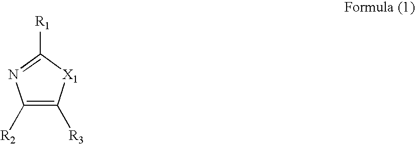
[0244]Electrochromic compound EC-1 [bis-(2-phosphonoethyl)-4,4′-bipyridium dibromide] was dissolved in acetonitrile / ethanol at 3 mmol / l to prepare ink liquid 5.

[0245](Preparation of Ink Liquid 6)

[0246]Exemplified compound (1)-26 was dissolved in acetonitrile / ethanol ...

example 3

[0278]The electrodes, inks, and electrolytic liquids obtained in Examples 1 and 2 were also used in Example 3 in the same manner.

[0279]>

[0280](Production of Display Element 3-1)

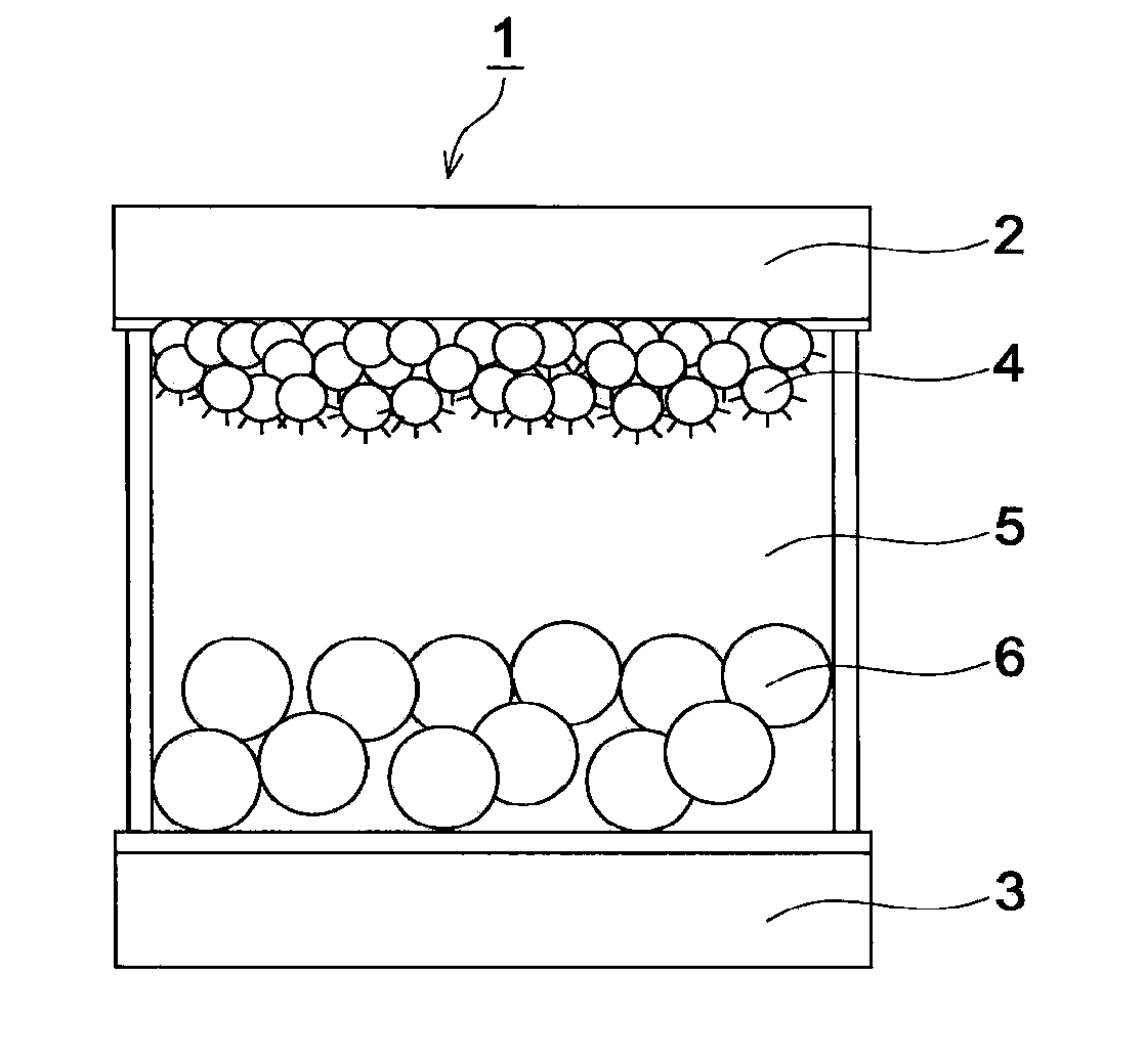
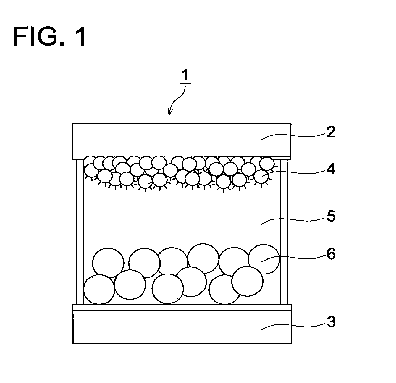
[0281]A mixed liquid, prepared by adding 20% by mass of titanium dioxide CR-90 (produced by Ishihara Sangyo Kaisha, Ltd.) in an isopropanol solution containing polyvinyl alcohol (average polymerization degree: 3500 and saponification degree: 87%) at 2% by mass, followed by being dispersed using an ultrasonic homogenizer, was coated on electrode 3 whose peripheral portion was edged with an olefin sealant containing a glass-made spherical bead spacer of an average particle diameter of 40 μm at a volume fraction of 10% to allow film thickness after drying to be 20 μm. Thereafter, drying was carried out at 15° C. for 30 minutes to evaporate the solvent and then further drying was carried out under an ambience of 45° C. for 1 hour.

[0282]A glass-made spherical bead spacer of an average particle diameter of 20 μm wa...


PUM

PropertyMeasurementUnit
reflectanceaaaaaaaaaa
operating voltageaaaaaaaaaa
voltageaaaaaaaaaa

Abstract

A display element containing at least 1 type of electrochromic compound, which is reversibly subjected to coloration or decoloration by at least either of electrochromic oxidation and reduction reaction, and an electrolyte between a pair of a display electrode and an opposed electrode; and undergoing a color tone change by an electrode driving operation, wherein a compound represented by following Formula (1) is held on the opposed electrode.

Description

TECHNICAL FIELD[0001]The present invention relates to a newly developed electrochromic display element.BACKGROUND[0002]Over recent years, with enhancement of operation speed of personal computers, widespread use of network infrastructure, and realization of mass storage of data, as well as cost reduction of data storage, there are increasing occasions in which information of documents and images, having been conventionally provided in the form of paper printed matter, is received and viewed as more convenient electronic information.[0003]As viewing methods for these items of electronic information, there are mainly used those which are of light emitting types such as conventional liquid crystal displays and CRTs, or organic EL displays, which have recently been marketed. Especially, however, when electronic information is composed of pieces of document information, it is necessary to stare at these viewing devices for a relatively long period of time, which is certainly not viewer-f...

Claims


Application Information

Patent Timeline
Patent Type & Authority Applications(United States)
IPC IPC(8): G02F1/153G02F1/1506
CPCG02F2001/1504G02F1/1506G02F2001/15025
Inventor ONO, KAORIISHIGE, OSAMUHAKII, TAKESHIHISAMITSU, AKIHITO
Owner KONICA MINOLTA INC
Why Eureka
Try Eureka