Polythiophenes and electronic devices comprising the same

a technology of polythiophene and electronic devices, applied in the direction of non-metal conductors, conductors, organic conductors, etc., can solve the problems of high silicon-based tft circuit costs, high cost of silicon-based tft circuits, and high cost of high-performance organic semiconductors. to achieve the effect of eliminating chlorinated solvents

Active Publication Date: 2010-06-10
SAMSUNG ELECTRONICS CO LTD
View PDF10 Cites 3 Cited by
  • Summary
  • Abstract
  • Description
  • Claims
  • Application Information

AI Technical Summary

Benefits of technology

[0008]It would be desirable to eliminate chlor

Problems solved by technology

TFT circuits using current mainstream silicon technology may be too costly for some applications, particularly for large-area electronic devices such as backplane switching circuits for displays (e.g., active matrix liquid crystal monitors or televisions) where high switching speeds are not essential.
The high costs of silicon-based TFT circuits are primarily due to the use of capital-intensive silicon manufacturing facilities as well as complex high-temperature, high-vacuum photolithographic fabrication processes under strictly controlled environments.
Most high-performance organic semiconductors suff

Method used


Image

  • Polythiophenes and electronic devices comprising the same
  • Polythiophenes and electronic devices comprising the same
  • Polythiophenes and electronic devices comprising the same

Examples


example 1

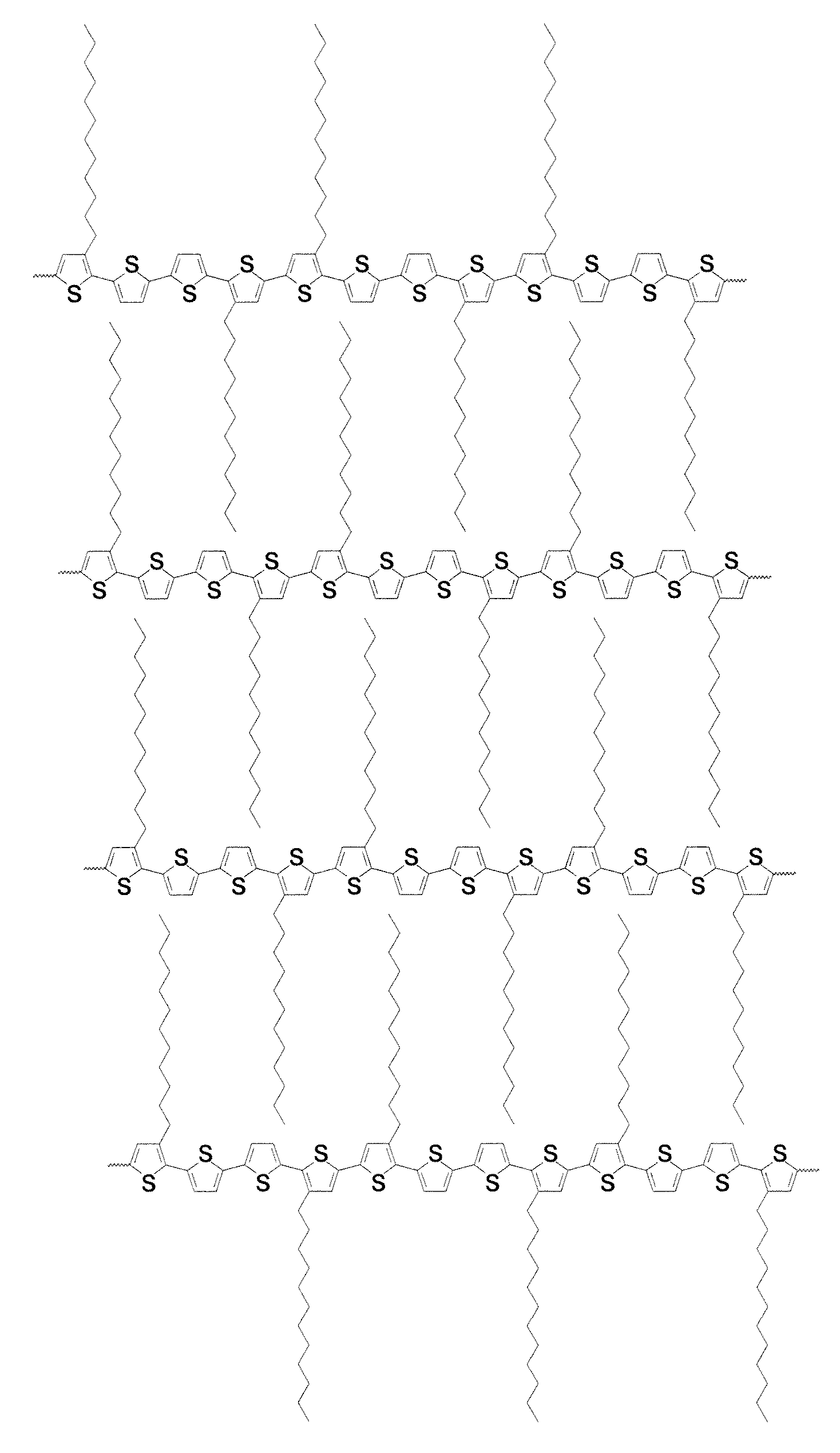
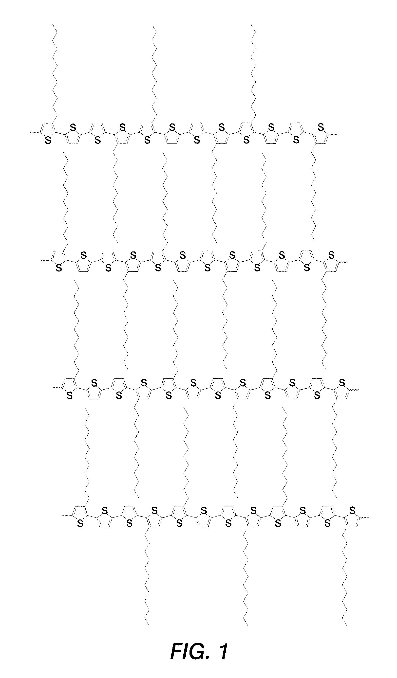
[0058]Poly[5,5′-bis(3-dodecyl-2-thienyl)-3-methyl-2,2′-dithiophene] was prepared as described in Scheme 1. This polythiophene corresponds to Polythiophene 1 of Scheme 1 set forth above.

[0059]Preparation of Monomer:

[0060]A solution of 2-bromo-3-dodecylthiophene (15.36 grams, 46.36 mmol) in 30 milliliters of anhydrous tetrahydrofuran (THF) was added slowly over a period of 20 minutes to a magnetically stirred suspension of magnesium turnings (1.69 grams, 69.52 mmol) in 10 milliliters of THF in a 250 milliliter round-bottomed flask under an inert argon atmosphere. The resultant mixture was stirred at room temperature for 2.5 hours, and then at 50° C. for 30 minutes before cooling down to room temperature.

[0061]The resulting fresh prepared Grignard reagent, 3-dodecyl-2-thiophenemagnesium bromide, was then added via a cannula to a mixture of 5,5′-dibromo-3-methyl-2,2′-dithiophene (6.27 grams, 18.54 mmol) and Ni(dppe)Cl2 (0.48 gram, 0.91 mmol) in 50 milliliters of anhydrous THF in a 250 m...

example 2

[0065]Three copolythiophenes were prepared according to Scheme 2 as set forth above. Monomer 2 was prepared by the method described in U.S. Pat. No. 6,770,904. Monomer 1 was prepared by the method described in Example 1.

[0066]For Copolythiophene 2a, x=90 mole % and y=10 mole %.

[0067]For Copolythiophene 2b, x=80 mole % and y=20 mole %.

[0068]For Copolythiophene 2c, x=50 mole % and y=50 mole %.

[0069]For Copolythiophene 2a, a solution of mixed 5,5′-bis(3-dodecyl-2-thienyl)-2,2′-dithiophene (Monomer 2) (500 mg, 0.75 mmol) and 5,5′-bis(3-dodecyl-2-thienyl)-3-methyl-2,2′-dithiophene (Monomer 1) (57 mg, 0.084 mmol) in 10 milliliters of chlorobenzene was added slowly over a period of about 5 minutes to a well stirred mixture of FeCl3 (500 mg, 3.08 mmol) in 5 milliliters of chlorobenzene in a 100 milliliter round-bottomed flask in an inert argon atmosphere. This mixture was stired at 60° C. for 48 hours. After the polymerization, the mixture was diluted with 50 milliliters of methylene chlori...


PUM

PropertyMeasurementUnit
Molecular weightaaaaaaaaaa
Semiconductor propertiesaaaaaaaaaa
Mobilityaaaaaaaaaa

Abstract

Disclosed are semiconducting polythiophenes comprising a repeating unit of Formula (A) or a copolythiophene of Formula (B):
wherein A and B are each alkyl having from 1 to about 25 carbon atoms; and a, b, c, d, e, f, g, x, and y are as defined herein. These polythiophenes have high mobility and are soluble in common organic solvents, so that chlorinated solvents do not need to be used. They are useful for depositing semiconducting layers, particularly in organic thin-film transistors.

Description

BACKGROUND[0001]The present disclosure relates, in various embodiments, to compositions and processes suitable for use in electronic devices, such as thin film transistors (“TFT”s). The present disclosure also relates to components or layers produced using such compositions and processes, as well as electronic devices containing such materials.[0002]Thin film transistors (TFTs) are fundamental components in modern-age electronics, including, for example, sensors, image scanners, and electronic display devices. TFT circuits using current mainstream silicon technology may be too costly for some applications, particularly for large-area electronic devices such as backplane switching circuits for displays (e.g., active matrix liquid crystal monitors or televisions) where high switching speeds are not essential. The high costs of silicon-based TFT circuits are primarily due to the use of capital-intensive silicon manufacturing facilities as well as complex high-temperature, high-vacuum p...

Claims


Application Information

Patent Timeline
IPC IPC(8): C08G75/02H01B1/12
CPCC08G61/126C08G2261/1412C08G2261/364C08G2261/51H01L51/0558H01B1/127H01L51/0036H01L51/0068C08G2261/92H10K85/113H10K85/655H10K10/484
Inventor LIU, PINGWU, YILIANGLI, YUNING
Owner SAMSUNG ELECTRONICS CO LTD
Why Eureka
Try Eureka