Chalcogenide nanoionic-based radio frequency switch

a radio frequency switch and nano-ionic technology, applied in the field ofchalcogenide nano-ionic based radio frequency switches, can solve the problems of high cost, solid-state diodes, complicated manufacturing processes of mems devices, etc., and achieve the effects of low cost, low insertion loss, and easy fabrication

Inactive Publication Date: 2010-06-10
NASA
View PDF40 Cites 9 Cited by
  • Summary
  • Abstract
  • Description
  • Claims
  • Application Information

AI Technical Summary

Benefits of technology

[0035]It is a further object of the invention to provide nanoscale electrochemical switches at low cost which are easy to fabricate.
[0036]It is a further object of the invention to provide electrochemical switches having low insertion loss in the “on” state (closed switch) and high power isolation in the “off” state (open switch).
[0037]It is a further object of the invention to provide a nonvolatile nanoionic switch which once energized with sufficient direct current voltage for a sufficient amount of time and with the positive voltage applied to the oxidizable electrode (anode) and the negative voltage applied to the inert electrode (cathode) requires no further energy to sustain the nanoionic switch in the closed position so that it may pass control signals of sufficiently high frequency having sufficiently low (root mean square) alternating current voltage.

Problems solved by technology

MEMS or solid-state based switches which are currently used are incapable of meeting future demands due to associated disadvantages.
MEMS devices utilize complicated manufacturing processes and are expensive to make.
Radio frequency switching applications usually employ solid state switches (i.e., diodes, FETs) or microelectromechanical systems (MEMS), both of which possess associated weaknesses.
Solid state diodes can be produced cost-effectively to operate at low voltages (1-3V) and high speeds (ns), but suffer from higher insertion loss, high DC power consumption, low isolation, and the generation of third-order harmonics / intermodulation distortion (IMD).
MEMS-based switches provide low insertion loss (˜0.2 dB), low DC power consumption (˜pW), high isolation (>30 dB), and good IMD performance, but exhibit reliability problems (e.g., stiction, moving parts), slower switching speeds (ps), high actuation voltages (5-50V) which require complex circuitry, and relatively complicated processing steps.
Furthermore, MEMS packaging presents additional problems which need to be addressed before widespread use is realizable.

Method used


Image

  • Chalcogenide nanoionic-based radio frequency switch
  • Chalcogenide nanoionic-based radio frequency switch
  • Chalcogenide nanoionic-based radio frequency switch

Examples


Embodiment Construction

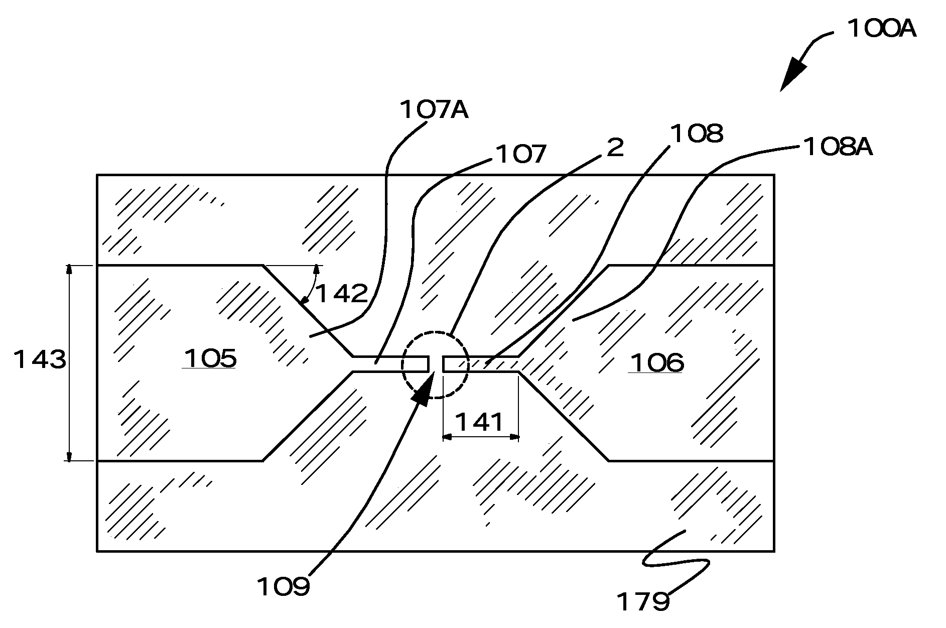
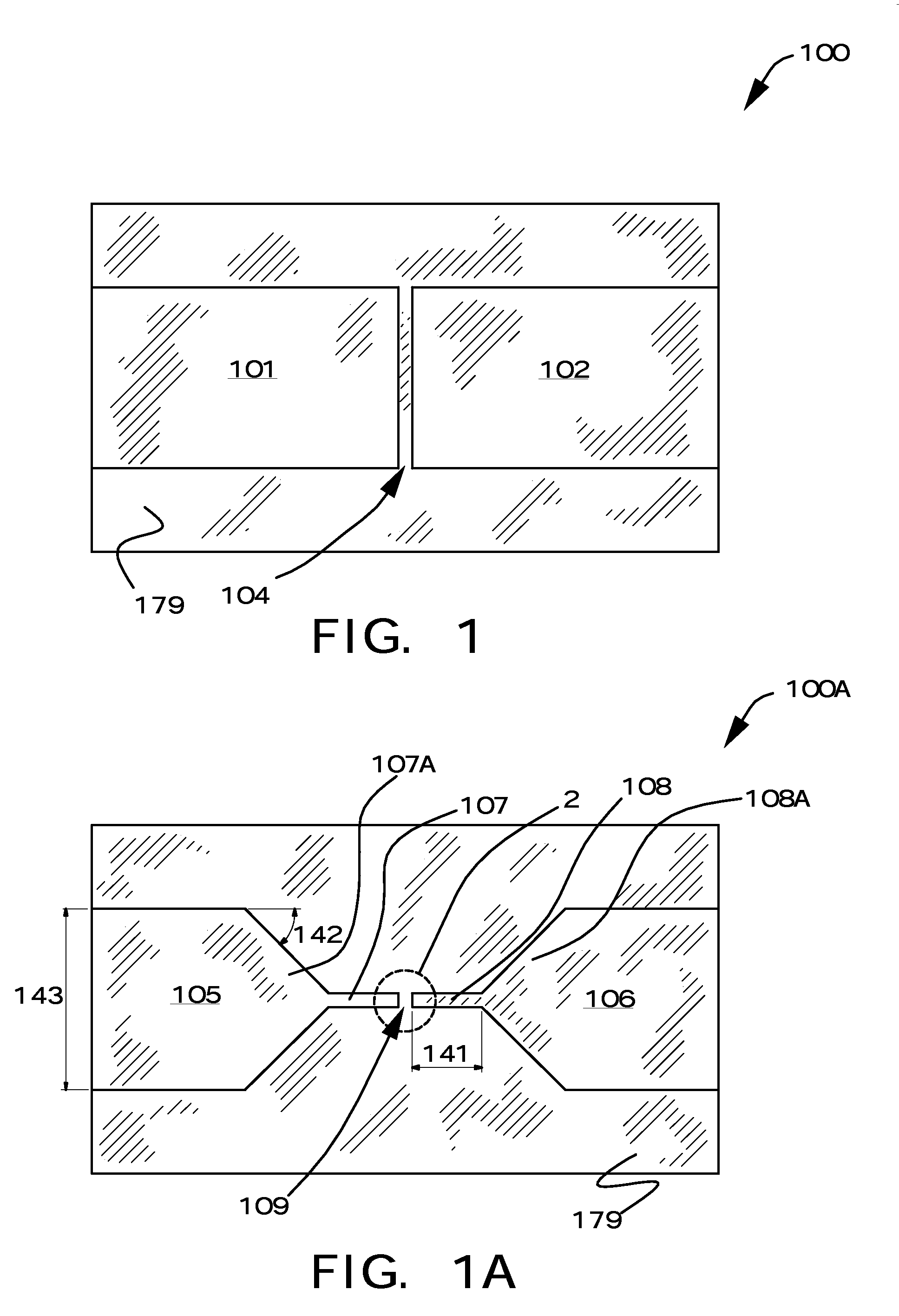
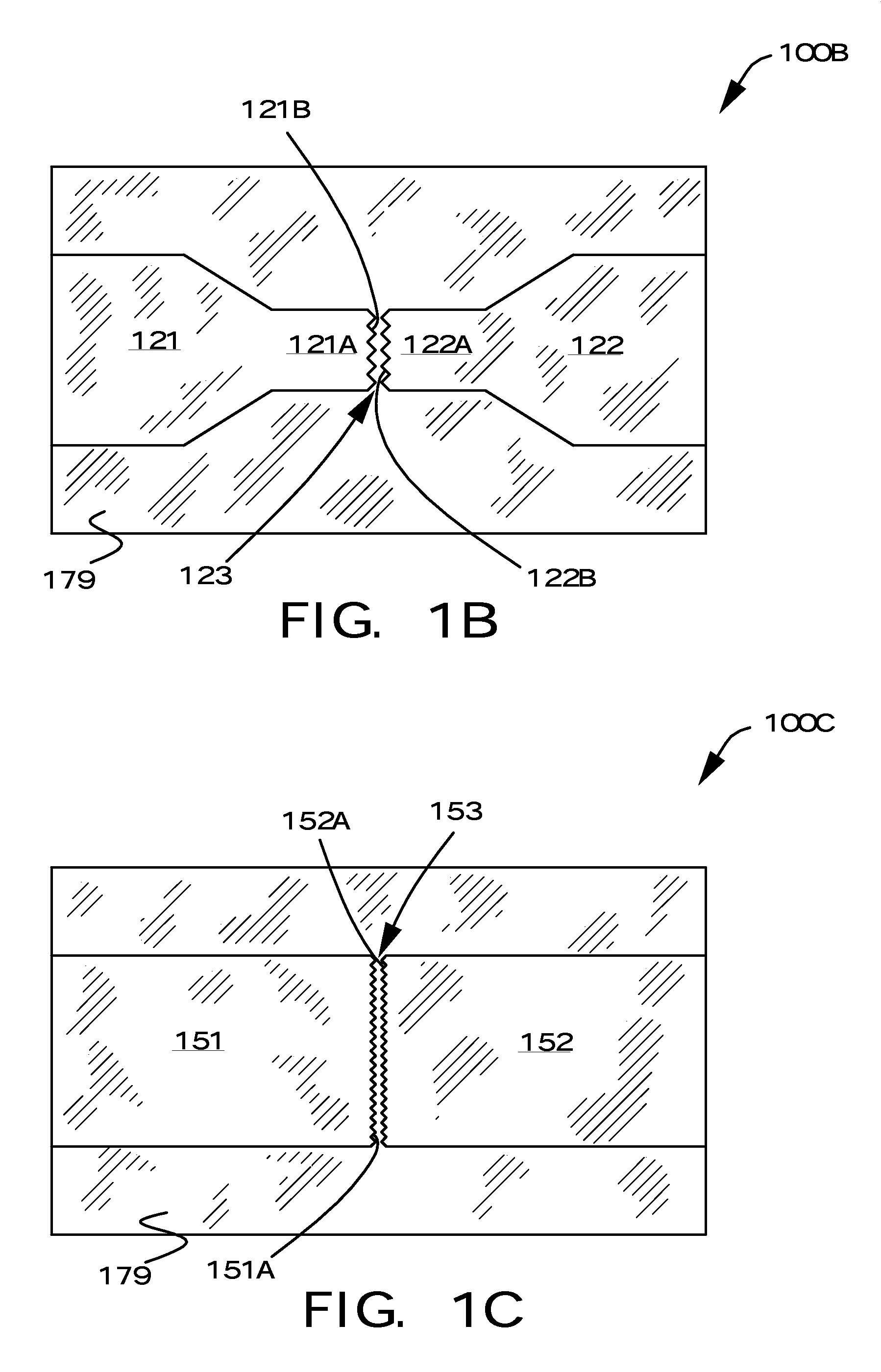
[0065]The fabrication of the nanoionics-based switch is described. A substrate (for example, having high resistivity (>1000 Ohm / cm silicon wafer) is deposited with a layer of binary chalcogenide glass (Col. IV and Col. VI element of the periodic table, e.g., Ge—Se, Ge—S, Si—O). Next, a layer of silver is deposited atop the glass and exposed to ultra violet light to induce a photo-dissolution process. Silver ions migrate into the glass matrix providing the framework for ionic transport and the capability of switching between a low-loss “on” state and a high isolation “off” state. Electrodes of dissimilar metals, one silver (oxidizable) and one inert (e.g., nickel) are deposited atop the chalcogenide layer to complete the switch. The switch also includes a passivation layer to protect it from the environment.

[0066]The electrochemical resistance-change process requires very little energy. Electrolytes are formed in a two step process in which a binary (Ge—Se, Ge—S, Si—O) base glass is ...


PUM

PropertyMeasurementUnit
current voltageaaaaaaaaaa
thickaaaaaaaaaa

Abstract

A nonvolatile nanoionic switch is disclosed. A thin layer of chalcogenide glass engages a substrate and a metal selected from the group of silver and copper photo-dissolved in the chalcogenide glass. A first oxidizable electrode and a second inert electrode engage the chalcogenide glass and are spaced apart from each other forming a gap therebetween. A direct current voltage source is applied with positive polarity applied to the oxidizable electrode and negative polarity applied to the inert electrode which electrodeposits silver or copper across the gap closing the switch. Reversing the polarity of the switch dissolves the electrodeposited metal and returns it to the oxidizable electrode. A capacitor arrangement may be formed with the same structure and process.

Description

FIELD OF THE INVENTION[0001]The invention is in the field of chalcogenide nanoionic based radio frequency switches.BACKGROUND OF THE INVENTION[0002]Radio frequency switches are basic building blocks for communication and control systems and are used for multiplexing of signals to achieve system reconfigureability and dynamic control. Radio frequency switches may be used in such applications as portable / mobile / satellite communication systems (e.g. cell-phones, PDAs, laptops, phased array antennas, sensors, tranceivers etc.). As communication systems approach higher data rate (Giga Bytes per second) and multi-functional operation, stringent requirements are placed on radio frequency switches. Some of these requirements include low power consumption, high reliability, high switching speed, high isolation, low insertion losses, ease of integration / implementation, as well as affordability. In particular, for 3 G (third generation) wireless phones and space-based applications, low power c...

Claims


Application Information

Patent Timeline
Patent Type & Authority Applications(United States)
IPC IPC(8): H01L47/00
CPCH01L45/00H10N70/245H10N70/823H10N70/8416H10N70/8822H10N70/8825H10N70/883H10N70/046H10N70/00
Inventor NESSEL, JAMESLEE, RICHARD
Owner NASA
Why Eureka
Try Eureka