Power semiconductor device and the method of manufacturing the same

a technology of semiconductor devices and manufacturing methods, applied in the direction of semiconductor devices, basic electric elements, electrical apparatus, etc., can solve the problems of insufficient injection enhancement effect, large turnoff loss, and long manufacturing process for manufacturing the conventional trench-gate structure, etc., to facilitate exhibiting high ie effects, reduce manufacturing costs, and facilitate manufacturing. high

Active Publication Date: 2010-06-10
FUJI ELECTRIC CO LTD
View PDF6 Cites 5 Cited by
  • Summary
  • Abstract
  • Description
  • Claims
  • Application Information

AI Technical Summary

Benefits of technology

[0021]The semiconductor device according to the invention is manufactured with very low manufacturing costs and with a high throughput of non-defective products. The semiconductor device according to the invention facilitates exhibiting high IE effects, exhibiting a low ON-state voltage, preventing electric field localization from causing and obtaining a high breakdown voltage.

Problems solved by technology

Since the turnoff proceeds more slowly as the ON-state voltage is lower, a larger turnoff loss is caused.
In other words, the IE effect (injection enhancement effect) obtained in the IGBT so far is insufficient.
The manufacturing process for manufacturing the conventional trench-gate structure is longer and more complicated than the manufacturing process for manufacturing the planar-gate structure.
The manufacturing costs for the conventional trench-gate structure tend to be higher than the manufacturing costs for the planar-gate structure.
In order to make the cell structure more minute and meticulous to further improve the device characteristics, the manufacturing costs will soar even higher.
In the IGBT having the conventional trench-gate structure, the electric field is liable to localize to the trench bottom and avalanche breakdown is caused easily.
Therefore, the breakdown voltage of the IGBT having the conventional trench-gate structure generally is liable to decrease.

Method used


Image

  • Power semiconductor device and the method of manufacturing the same
  • Power semiconductor device and the method of manufacturing the same
  • Power semiconductor device and the method of manufacturing the same

Examples


first embodiment

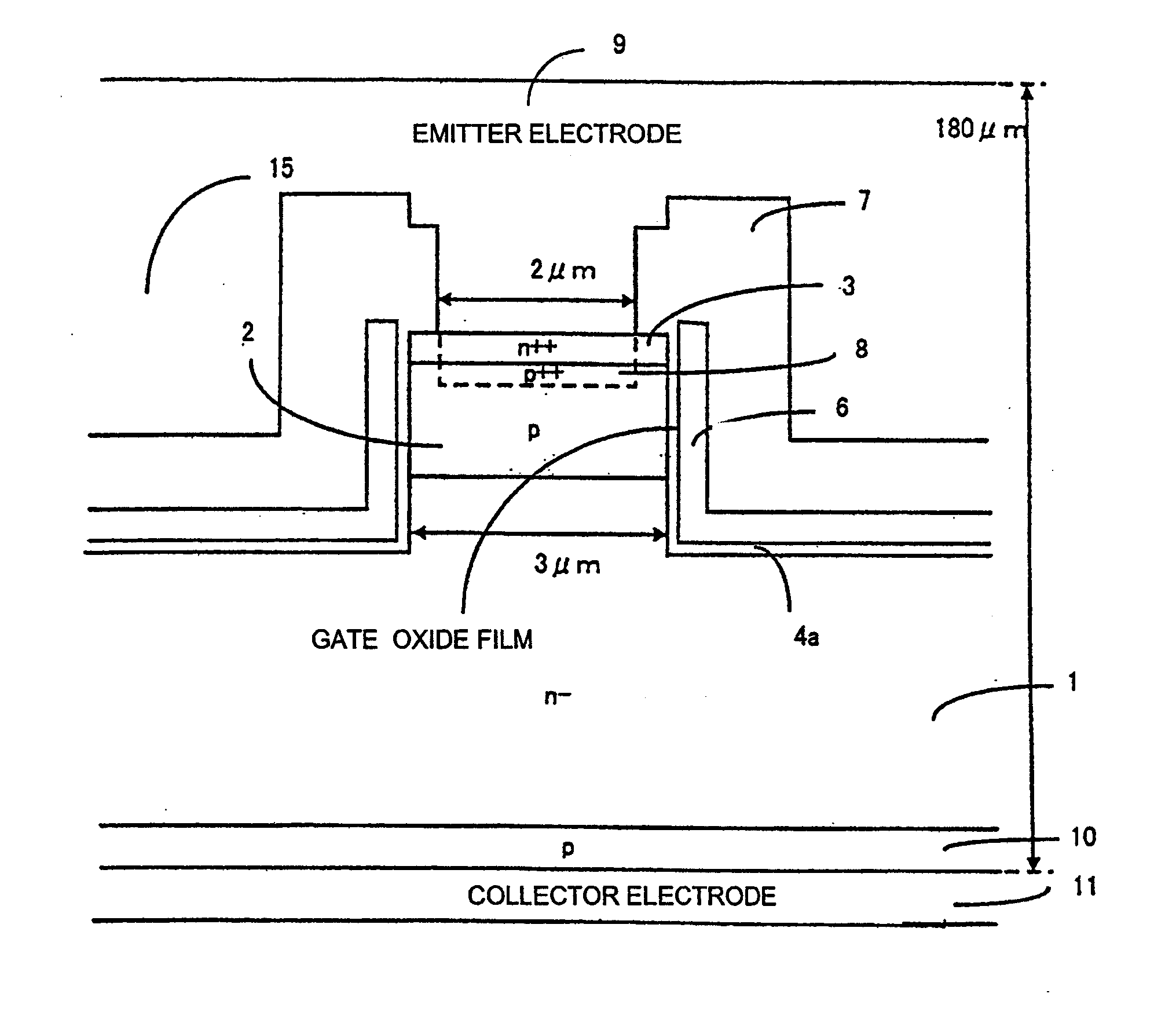
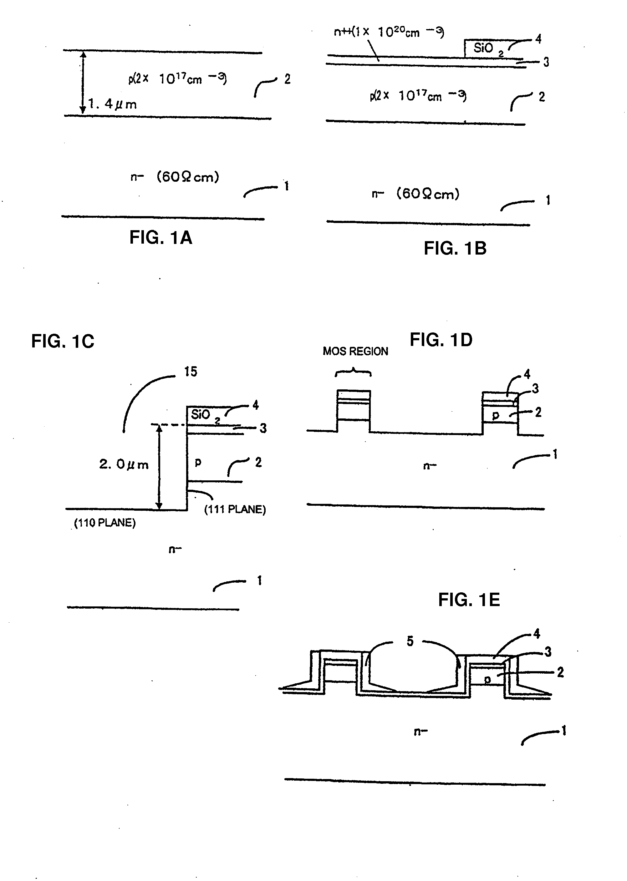
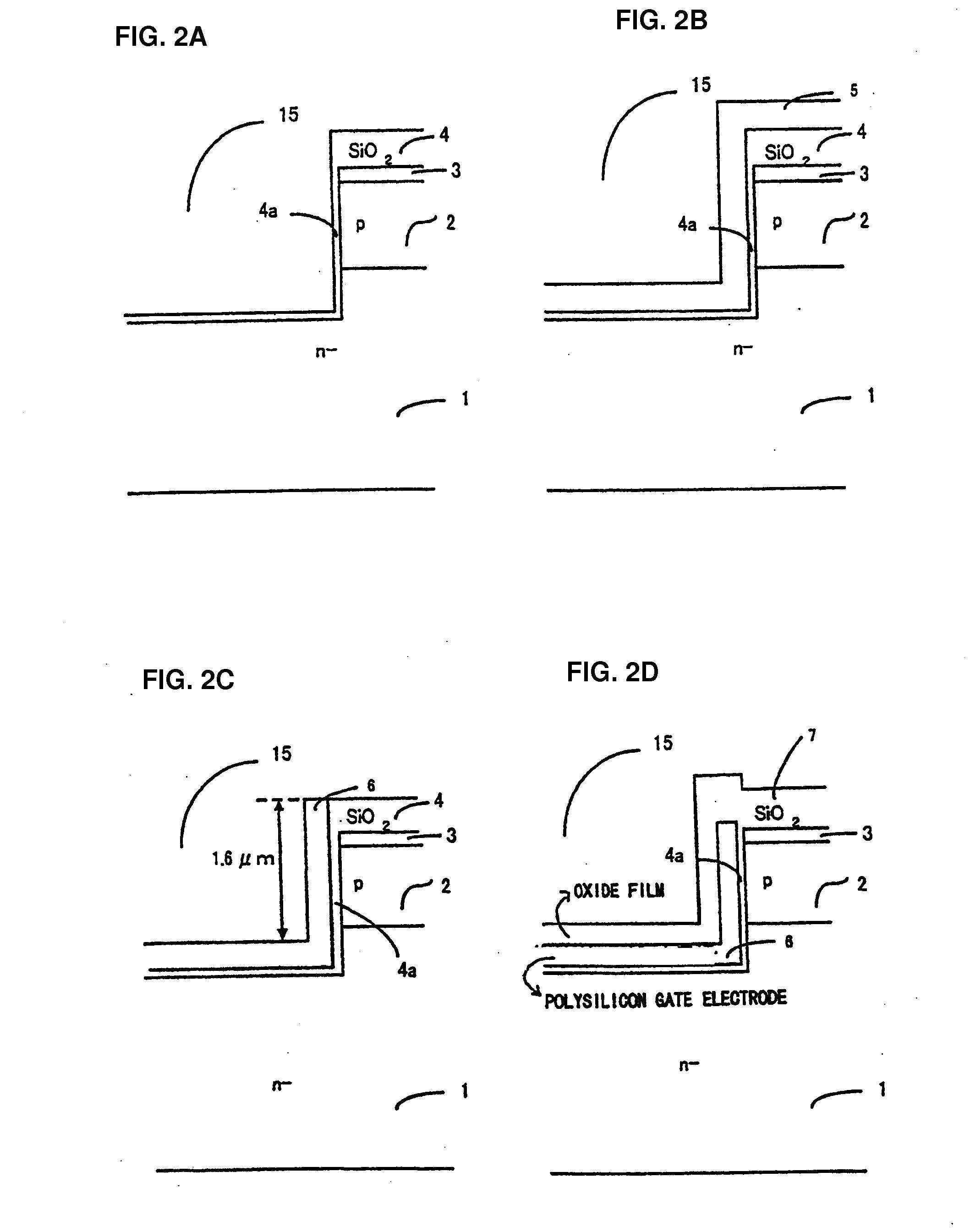
[0054]FIGS. 1A, 1B, 1C, 1D, 1E, 2A, 2B, 2C, 2D, 3A, 3C, 3D, and 4 are cross sectional views of a semiconductor wafer describing the main manufacturing steps for manufacturing a non-punch-through IGBT exhibiting a rated breakdown voltage of 1200 V (hereinafter referred to as a “1200V-NPT-IGBT”) according to a first embodiment of the invention. FIG. 3B is a plan view of the semiconductor wafer describing the main manufacturing step for manufacturing the 1200V-NPT-IGBT according to the first embodiment.

[0055]Now the manufacturing steps for manufacturing the 1200V-NPT-IGBT according to the first embodiment will be described below with reference to these drawings. Referring first to FIG. 1A, n-type FZ silicon substrate 1, having a (100) major surface and exhibiting the resistivity of 60 Ωcm, is prepared as the starting material. The n-type FZ silicon substrate 1 will serve as n−-type drift layer 1. At first, trichlorosilane, diborane, and hydrogen are fed to an epitaxial growth furnace. ...

second embodiment

[0073]FIGS. 5A, 5B, 5C, 5D, 6A, 6B, 6C, 7A, 7B, 9A and 9B are cross sectional views of a semiconductor wafer describing the main manufacturing steps for manufacturing a NPT-IGBT, the rated breakdown voltage thereof is 600V, (hereinafter referred to as a “600V-NPT-IGBT”) according to a second embodiment of the invention. FIGS. 6D, 8A and 8B are plan views of the semiconductor wafer describing the main manufacturing steps for manufacturing the 600V-NPT-IGBT according to the second embodiment.

[0074]Now the manufacturing steps for manufacturing the 600V-NPT-IGBT according to the second embodiment will be described below with reference to these drawings.

[0075]Referring at first to FIG. 5A, n-type FZ silicon substrate 101, having a (100) major surface and exhibiting the resistivity of 30 Ωcm, is prepared as a starting material. Thermal oxide film 100, 2.0 μm thick, is grown by pyrogenic oxidation at 1150° C. for 13 hours. Alternatively, an oxide film, 2.0 μm thick, may be grown by chemica...

third embodiment

[0115]FIGS. 15A, 15B, 16A, 17A, 18A, and 18B are cross sectional views of a semiconductor wafer describing the main manufacturing steps for manufacturing a field-stop-type IGBT exhibiting a rated breakdown voltage of 1200V (hereinafter referred to as a “1200V-FS-IGBT”) according to a third embodiment of the invention. FIGS. 17B and 19A are plan views of a semiconductor wafer describing the main manufacturing steps for manufacturing the 1200V-FS-IGBT according to the third embodiment. FIGS. 16B, 19B, 20, 21, and 22 are explanatory drawings, each including a top plan view and cross sectional views of a semiconductor wafer, for describing the main manufacturing steps for manufacturing the 1200V-FS-IGBT according to the third embodiment.

[0116]Now the manufacturing steps for manufacturing the 1200V-FS-IGBT according to the third embodiment of the invention will be described below with reference to these drawings.

[0117]Referring now to FIG. 15A, n-type FZ silicon substrate 201, having a (...


PUM


Abstract

A semiconductor device according to the invention includes n-type semiconductor substrate 1; trenches 15 formed in the surface portion of semiconductor substrate 1; a protruding semiconductor region between trenches 15; p-type base layer 2 in the protruding semiconductor region, p-type base layer 2 being positioned as deep as or shallower than trench 15; an n++-type emitter region or a source region in the surface portion of p-type base layer 2; gate insulator film 4a on the first side wall of the protruding semiconductor region; and gate electrode 6 on gate insulator film 4a. Trench 15 is from 0.5 μm to 3.0 μm deep and the short side of trench 15 is 1.0 μm or longer. The short side of the protruding semiconductor region is from 0.5 μm to 3.0 μm long. Gate electrode 6 contains electrically conductive polycrystalline silicon as its main component. Gate electrode 6 is from 0.2 μm to 1.0 μm thick. The semiconductor device according to the invention is manufactured with very low manufacturing costs and with a high throughput of non-defective products. The semiconductor device according to the invention facilitates exhibiting a high IE effects, exhibiting a low ON-state voltage, preventing electric field localization from causing and realizing a high breakdown voltage.

Description

BACKGROUND OF THE INVENTION[0001]A. Field of the Invention[0002]The present invention relates to a power semiconductor device used in electric power converters. Specifically, the invention relates to an IGBT and such a MOS semiconductor device and the method of manufacturing the MOS semiconductor device.[0003]B. Description of the Related Art[0004]The performance of the IGBT has progressed through many improvements. It has been required for the IGBT in the OFF-state to sustain the voltage of the current to be controlled and to interrupt the current to be controlled perfectly. It has been required for the IGBT in the ON-state to make the current to be controlled flow with a voltage drop as low as possible, i.e., with small ON-state resistance, and to work as a switch that causes a low power loss.[0005]There exists a tradeoff relation between the maximum voltage that the IGBT can sustain, i.e., the breakdown voltage, and the voltage drop caused in the ON-state of the IGBT. In the IGBT...

Claims


Application Information

Patent Timeline
Patent Type & Authority Applications(United States)
IPC IPC(8): H01L29/739H01L21/331
CPCH01L29/0657H01L29/0839H01L29/7397H01L29/402H01L29/66348H01L29/1095
Inventor TAKEI, MANABU
Owner FUJI ELECTRIC CO LTD
Why Eureka
Try Eureka