Method of making foraminous microstructures

a microstructure and foraminous technology, applied in the field of foraminous, porous microstructures, can solve the problems of poor scalability, high cost, and limited application of photonic crystal fiber fabrication methods, and achieve the effect of improving the scalability and scalability of the material, and achieving the effect of improving the scalability and scalability

Inactive Publication Date: 2010-06-17
CITY UNIVERSITY OF HONG KONG
View PDF13 Cites 14 Cited by
  • Summary
  • Abstract
  • Description
  • Claims
  • Application Information

AI Technical Summary

Benefits of technology

[0006]The current invention provides a method of making a foraminous microstructure or film that can be made to exhibit photonic and plasmonic properties using well-established solution-based deposition and post-deposition modification techniques, without sophisticated and expensive vacuum equipment or control systems. More specifically, the invention provides for a method of making a foraminous microstructure, comprising forming a structure comprising at least two materials wherein a ratio between the two materials varies in a depth direction of the structure, and removing one of the materials from the structure.
[0010]The method of the invention can be used to achieve elaborate periodic microstructures with high structural precision and uniformity over a large area substrate (e.g., on centimeter scale or larger). The overall procedure is highly efficient and amenable to automatic fabrication for mass production. The method of the invention does not require flat substrate surface, but allows for the structure to be deposited on substrates with diverse geometrical features. The compositional profile of the structure deposition can be flexibly controlled and varied to achieve a specialized function such as color coded conductor / magnet, anti-reflection conductor / magnet, transparent conductor / magnet, and photovoltaic electrode materials with high-absorption at the entire solar wavelengths.

Problems solved by technology

The current major challenge in the fabrication of photonic structures is in creating structures with sufficient precision and good scalability.
These vapor deposition methods usually entail sophisticated and expensive vacuum equipment and control systems.
This technique does not entail vapor deposition processes, but is exclusively limited to the fabrication of photonic crystal fibers.
One widely used approach is based on sophisticated micro-fabrication methods derived from microelectronics and laser beam writing techniques; however, these methods are usually either labor-intensive, expensive or complex and are not commercially used.
However, electrochemical etching method only applies to single crystal semiconductor wafers, and the other methods are inconvenient to achieve for instance continuously modulating photonic structures with high resolution.
The colloidal self-assembly involves using self-assembled colloidal nanobeads as templates, however, this approach is subject to the structural defects inherent in the template, and lacks flexibility in designing structural features other than those molded by the closest packed nanobeads.

Method used


Image

  • Method of making foraminous microstructures
  • Method of making foraminous microstructures
  • Method of making foraminous microstructures

Examples


example

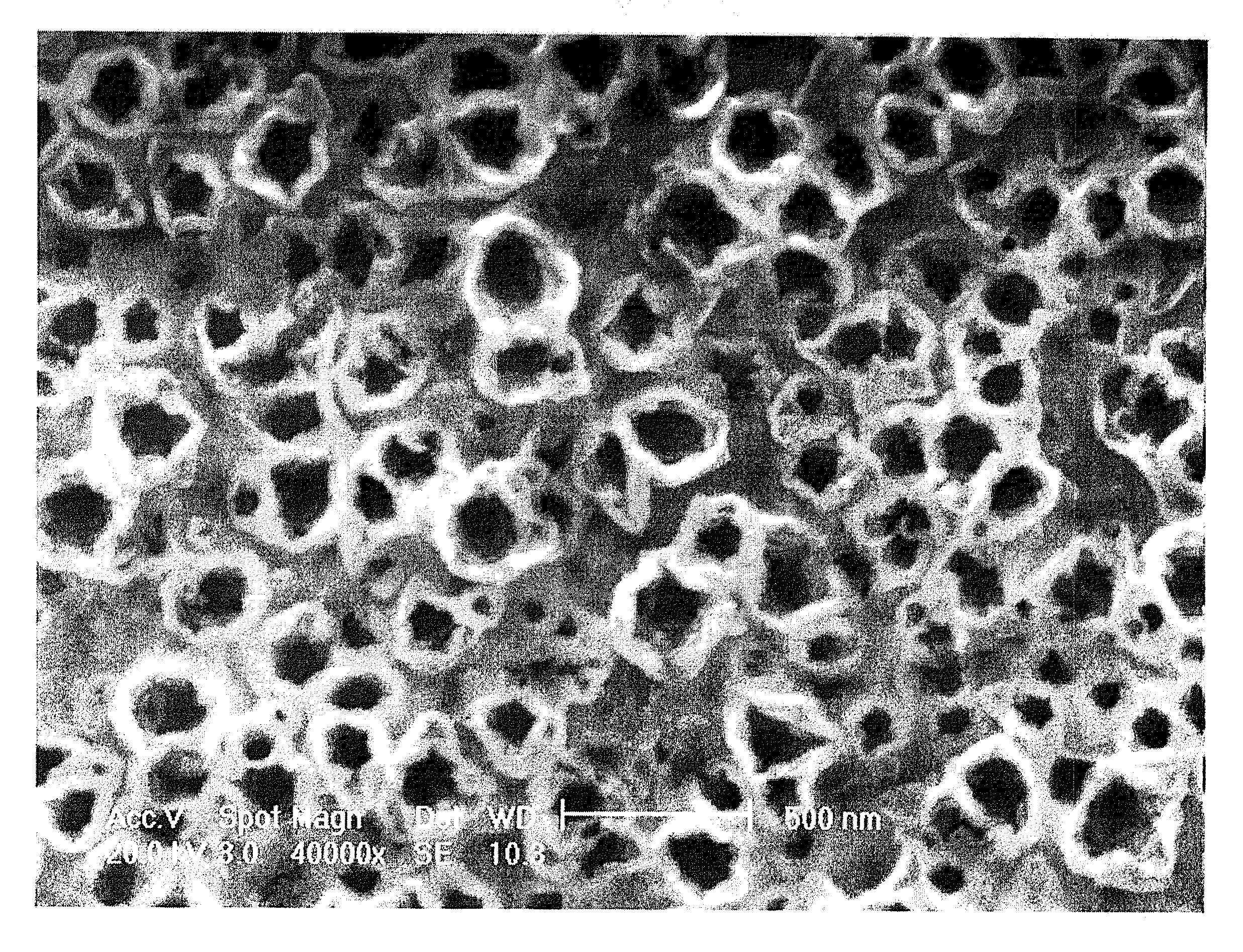
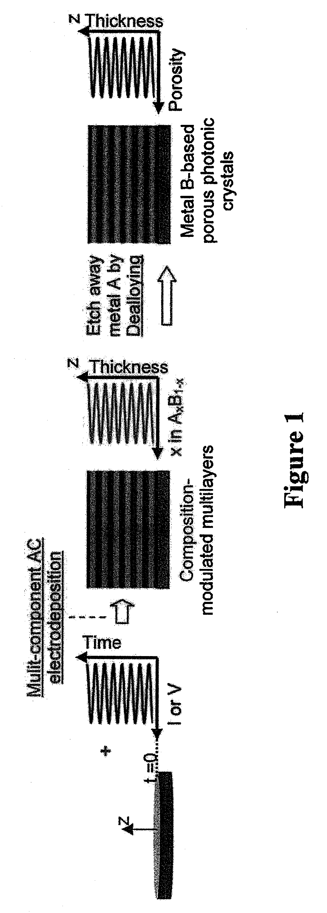
[0054]The invention is further illustrated by the following example. A Ni—Cu system is illustrated because it is among the best established electrodeposited multilayered systems, has interesting magnetic properties and is easily fabricated. A rugate mirror is further chosen to demonstrate the versatility and precision of the invented method, since the continuously modulated composition profile of a rugate filter together with the processing difficulty of metals have posed a great challenge for the current fabrication techniques. To demonstrate the precision of the method, a porous Ni-based multilayer film with each layer of 10 nm thickness is constructed.

[0055]A Ni—Cu multilayer film is grown by electrodeposition in a deposition solution containing 0.5 M nickel sulfamate (Ni(H2NSO3)2) and 0.05 M copper sulfate (CuSO4) buffered to pH 2.5 with boric acid (H3BO3). A typical three-electrode cell is used, with an ITO glass or Au coated Si wafer as the working electrode, a Pt spiral wires...


PUM

PropertyMeasurementUnit
sizeaaaaaaaaaa
thicknessaaaaaaaaaa
thicknessaaaaaaaaaa

Abstract

A foraminous microstructure or film that has photonic or plasmonic properties is made by forming a structure or film composed of at least two constituent materials so that the compositional ratio of the constituent materials varies in a depth direction of the structure, and then removing one of the materials from the structure.

Description

BACKGROUND OF THE INVENTION [0001]1. Field of the Invention[0002]The current invention relates to methods of making foraminous, or porous, microstructures, and in particular to methods of making foraminous films for use in photonic or plasmonic applications.[0003]2. Background Information[0004]The current major challenge in the fabrication of photonic structures is in creating structures with sufficient precision and good scalability. Hitherto man-made photonic structures have been fabricated by one of two commercial techniques. The first technique is based on a family of vapor deposition techniques for constructing photonic coatings on mirrors and lens. These vapor deposition methods usually entail sophisticated and expensive vacuum equipment and control systems. The other technique is the fiber draw technique. This technique does not entail vapor deposition processes, but is exclusively limited to the fabrication of photonic crystal fibers.[0005]Other non commercial methods for ph...

Claims


Application Information

Patent Timeline
Patent Type & Authority Applications(United States)
IPC IPC(8): B44C1/22
CPCB82Y20/00
Inventor LI, YANG YANGXU, ZHENGTAOTSANG, CHUN KWAN
Owner CITY UNIVERSITY OF HONG KONG
Why Eureka
Try Eureka