Semiconductor nanocrystals and preparation methods thereof

a technology of semiconductor nanocrystals and nanocrystals, which is applied in the field of semiconductor nanocrystals, can solve the problems of difficult synthesizing of group iii-v semiconductor nanocrystals, nanocrystals as well as their precursors, and environmental pollution problems

Active Publication Date: 2010-06-24
SAMSUNG ELECTRONICS CO LTD
View PDF5 Cites 60 Cited by
  • Summary
  • Abstract
  • Description
  • Claims
  • Application Information

AI Technical Summary

Benefits of technology

[0008]Disclosed herein is a nanocrystal, including a core including a Group III-V semiconductor and a transition metal alloyed with the Group III-V semicondu

Problems solved by technology

Group III-V semiconductor nanocrystals have recently attracted much attention in view of Group II-VI semiconductor nanocrystals, which can cause environmental pollution problems.
However, a Group III-V semiconductor nanocrystal, as well as its precursors, can be sensitive to oxygen and moisture during preparation.
Further, a Group III-V semiconductor nanocrystal

Method used


Image

  • Semiconductor nanocrystals and preparation methods thereof
  • Semiconductor nanocrystals and preparation methods thereof
  • Semiconductor nanocrystals and preparation methods thereof

Examples


example 1

Preparation of an InZnP Core and an InZnP / ZnS Nanocrystal

example 1-1

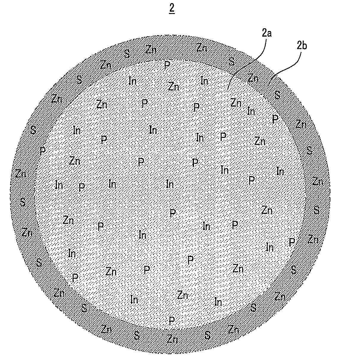
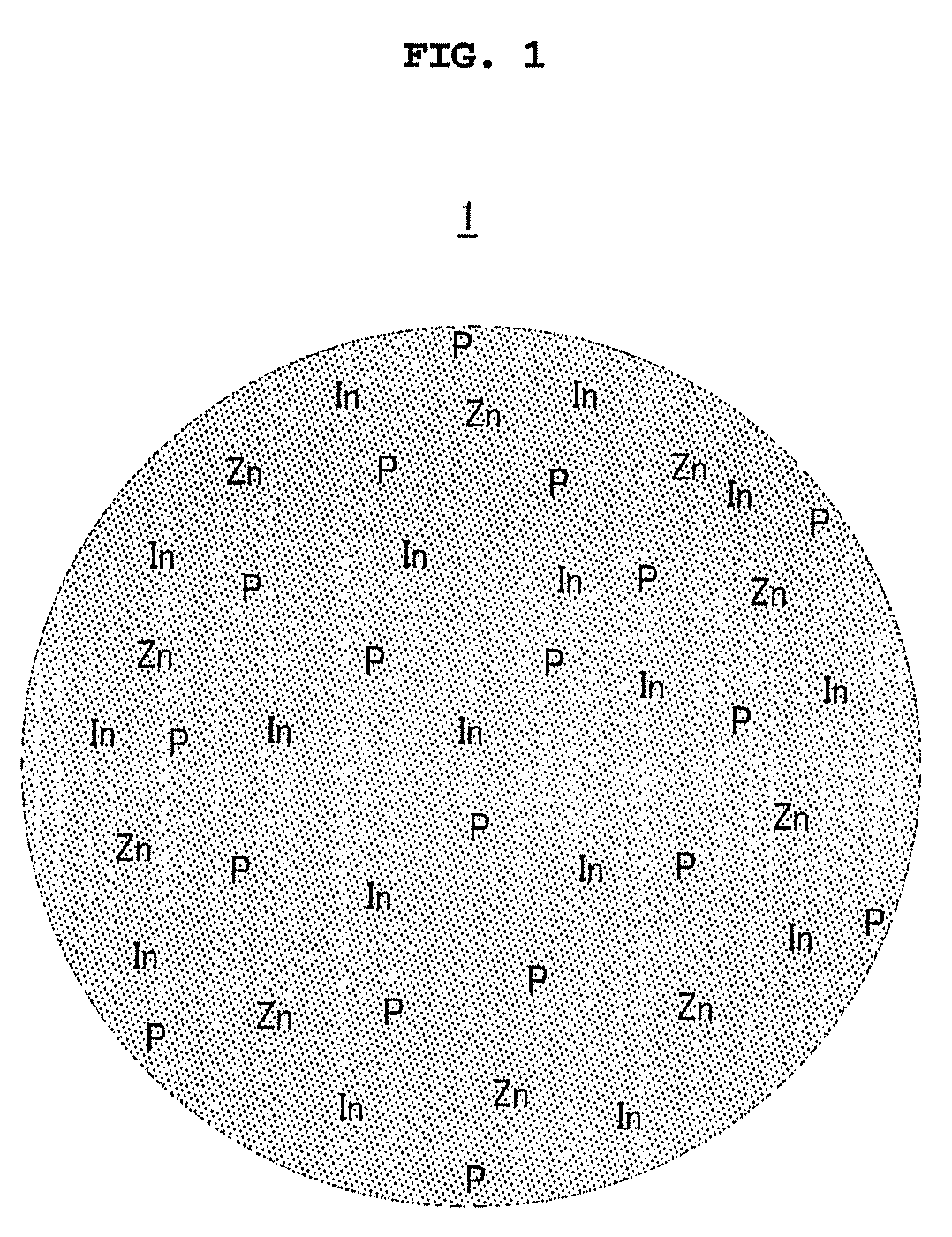
[0071]Indium acetate (0.2 millimoles (“mmol”) and zinc acetate (0.05 mmol) are added to a mixture of palmitic acid (0.7 mmol) and octadecene (10 milliliters “mL”), heated to 120° C. under vacuum, and maintained at 120° C. for one hour. The resulting mixture is heated to 280° C. under a nitrogen atmosphere, and then a solution of 0.1 mmol of trimethylsilyl-3-phosphine and 1 mL of trioctyl phosphine is injected into therein. After the injection, the solution is allowed to react for 2 minutes. The reaction solution is rapidly cooled to room temperature, which is less than 25° C., followed by acetone treatment to separate an InZnP core having an optical density of 0.1.

example 1-2

[0072]Zinc acetate (0.3 mmol) is added to a mixture of oleic acid (0.9 mmol) and octadecene (10 mL), heated to 120° C. under a vacuum and maintained at 120° C. for one hour. The resulting mixture is heated to 240° C. under a nitrogen atmosphere, and then 1.5 mL of a 0.4 M sulfur / trioctyl phosphine solution and 1 mL of the InZnP core prepared in Example 1-1 is injected therein. The mixture is heated to 280° C. and reacted for one hour. The reaction solution is cooled to room temperature, which is less than 25° C., to separate an InZnP / ZnS nanocrystal.


PUM

PropertyMeasurementUnit
Temperatureaaaaaaaaaa

Abstract

A nanocrystal includes a core including a Group III-V semiconductor and a transition metal alloyed with the Group III-V semiconductor, wherein the transition metal is present at a higher molar concentration in an outermost surface layer of the core than in a central portion of the core.

Description

CROSS-REFERENCE TO RELATED APPLICATION[0001]This application claims priority to Korean Patent Application No. 10-2008-130506, filed on Dec. 19, 2008, and all the benefits accruing therefrom under 35 U.S.C. § 119, the contents of which in its entirety are herein incorporated by reference.BACKGROUND[0002]1. Field[0003]The present disclosure is directed to semiconductor nanocrystals and methods for preparing the same. More specifically, the methods are related to the preparation of Group III-V semiconductor nanocrystals having controlled emission wavelength and improved color purity.[0004]2. Description of the Related Art[0005]A semiconductor nanocrystal, also called a “quantum dot,” is a crystalline semiconductor material having a size of a few nanometers and consisting of several hundred to several thousand atoms. A semiconductor nanocrystal has a large surface area per unit volume and exhibits various effects (e.g., quantum confinement) due to its small size. These structural charac...

Claims


Application Information

Patent Timeline
IPC IPC(8): H01B1/02B32B1/00
CPCC09K11/025C09K11/70H01L33/502Y10T428/2982H05B33/14Y10T428/2991H01L51/502H10K50/115B82B1/00B82B3/00
Inventor JANG, EUN JOOJUN, SHIN AEJANG, HYO SOOK
Owner SAMSUNG ELECTRONICS CO LTD
Why Eureka
Try Eureka