
Polishing pad and method of manufacturing the same

a technology of polishing pad and surface, which is applied in the field of polishing pad, can solve the problems of not allowing the magnetic head to fly properly, damage to the surface of the magnetic disk, and malfunction of reading and writing information, etc., and achieves excellent polishing performance, low occurrence of scratches, and favorable surface uniformity.

Inactive Publication Date: 2010-07-08
KOLON IND INC
View PDF1 Cites 4 Cited by
  • Summary
  • Abstract
  • Description
  • Claims
  • Application Information

AI Technical Summary

Benefits of technology

The present invention relates to a polishing pad for chemical mechanical polishing (CMP) processes, especially for high capacity and memory density integrated circuit chips. The polishing pad is effective in preventing close contact between the recording disk and magnetic head, reducing damage to the surface of the magnetic disk, and improving the polishing performance of the pad. The invention also provides a method for manufacturing the polishing pad that overcomes the problems of conventional methods, such as difficulty in controlling pore size and short product life. The technical effects of the invention include improved surface smoothness, reduced damage to the substrate, and improved polishing performance.

Problems solved by technology

Due to considerably decreased fly height, if a protrusion formed on a surface of a magnetic recording disk, the protrusion may contact a magnetic head to cause head crash, resulting in damage to the surface of the magnetic disk.
Also, even with a microfine protrusion substantially not causing the head crash, it may contact the magnetic head and possibly cause malfunction in reading and writing information.
Additionally, because of the protrusion, the magnetic head may be in close contact with the surface of the disk, causing a problem of not allowing the magnetic head to fly properly.
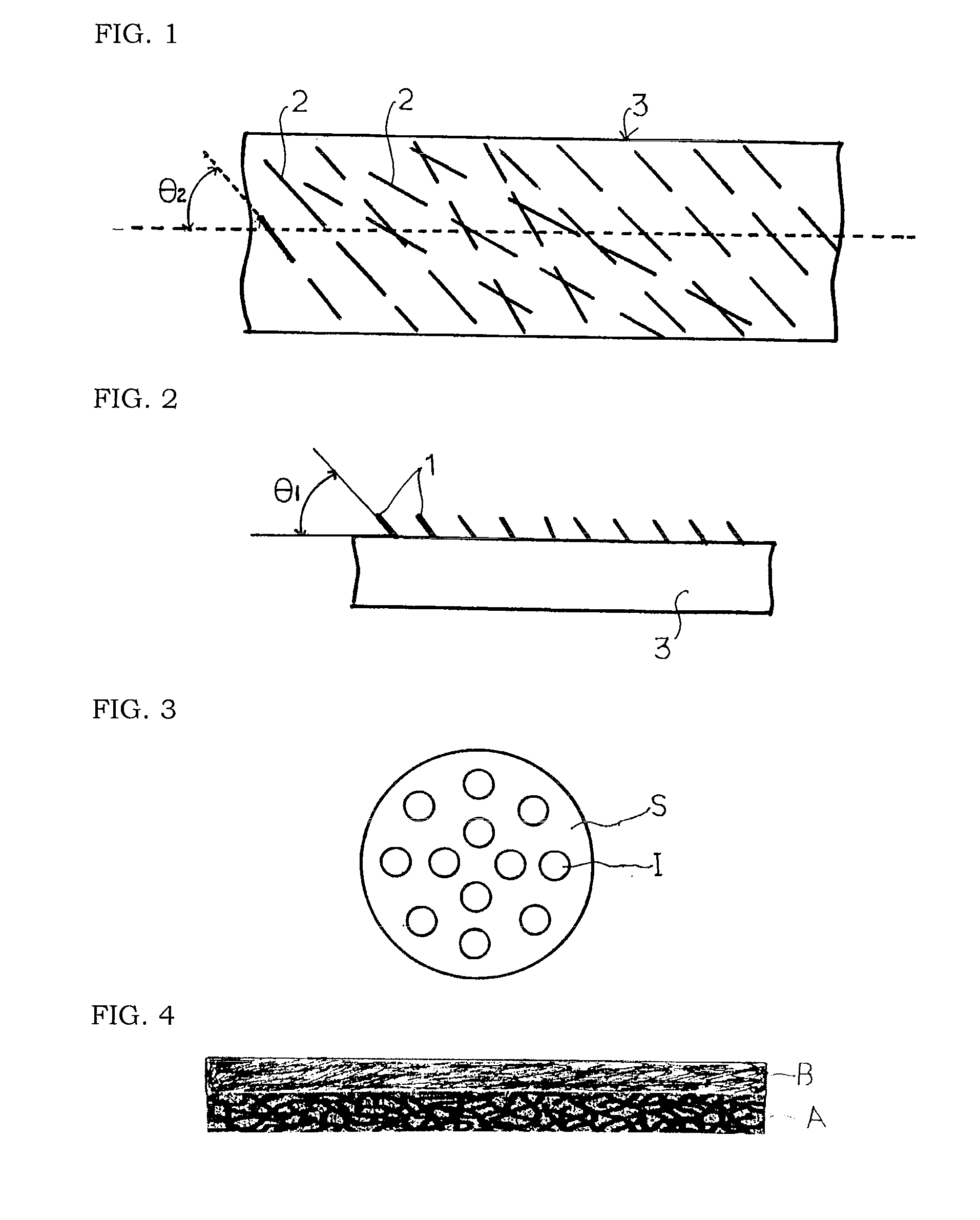
For this reason, the polishing pad described above needs composite processes and encounters a problem that it is difficult to uniformly control a size of pores in the coating layer B.
Furthermore, when the coating layer B is completely worn out, the polishing pad cannot be used any more even though the pad A under the coating layer B remains unchanged or unworn.
Therefore, this has problems of short product life and / or causing a great amount of waste of raw materials.
Such a polishing pad described above exhibits an irregular surface and has thick staple fibers arranged on the surface of the pad, thereby causing a lack of pores between the fibers and a decrease in polishing performance of the pad.
However, the ultrafine fibers arranged on the surface of the polishing pad are too much parallel in the longitudinal direction of the pad, that is, have a very small orientation angle θ2, as well as a fiber raising angle θ1 of the ultrafine fibers raised on the surface thereof so small that a binding force between bundles of ultrafine fibers is excessively high to deter slurry particles from smoothly flowing during the texturing process, resulting in agglomeration of the particles.
Therefore, the polishing pad disclosed in the above patent has disadvantages of reduced polishing performance and many scratches occurring on a polished surface of a magnetic recording medium.

Method used


Image

  • Polishing pad and method of manufacturing the same

Examples


example 2

[0115]A polishing pad was produced by the same procedure as in Example 1 except that the non-woven fabric prepared in Example 1 was firstly treated using an alkaline solution to extract a sea component S from the composite fiber and impregnated with 40% by weight of polyurethane resin relative to total weight of the fabric, followed by a wet coagulation method. Using the produced polishing pad, a silicon wafer with an area of 100 inch2 was polished by the same process as in Example 1.

[0116]Among the total amount of ultrafine fibers arranged on the surface of the polishing pad, the ratio of ultrafine fibers having an orientation angle θ2 in a range of 0 to 30° was determined. The results are shown in TABLE 1.

[0117]The polished silicon wafer was subjected to measurement of average surface roughness and scratch occurrence. The results are shown in TABLE 1.

example 3

[0124]An elution type composite fiber (a monofilament fineness for the polyamide fiber component: 0.05 denier) comprising an eluted component based on polyester copolymer, which reacts to divide a cross-section of a yarn into 32 segments, and a polyamide fiber component, which is divided by a slit component in the eluted component and has a cross-section in a triangle form, was cut into staple fibers having a length of 50 mm. After carding and cross-lapper processing, the treated staple fibers were formed into a laminate web. The laminate web was subjected to needling punching, resulting in a non-woven fabric made of the elution type composite fiber.

[0125]Next, the produced fabric was impregnated with 40% by weight of polyurethane resin relative to total weight of the fabric, then, treated by a wet coagulation method. The coagulated fabric was treated using an alkaline solution (such as sodium hydroxide) to obtain the eluted component from the composite fiber, followed by a fiber ra...

example 4

[0130]A split type composite fiber comprising polyester based radial components, which have a cross-section divided into segments by slit components, was cut into staple fibers having a length of 50 mm. After carding and cross-lapper processing, the treated staple fibers were formed into a laminate web. The laminate web was subjected to a needle punching process, resulting in a non-woven fabric made of the split type composite fiber.

[0131]Next, the produced fabric was impregnated with 40% by weight of polyurethane resin relative to total weight of the fabric, then, treated by a wet coagulation method. The coagulated fabric was treated using an alkaline solution (such as sodium hydroxide) to obtain an eluted component from the composite fiber, followed by a fiber raising treatment such that ultrafine fibers were raised on a surface of the fabric to produce a sheet type product comprising the non-woven fabric made of ultrafine fibers and impregnated with elastomeric polymer.

[0132]Afte...


PUM

PropertyMeasurementUnit
orientation angle θ2aaaaaaaaaa
orientation angleaaaaaaaaaa
orientation angle θ2aaaaaaaaaa

Abstract

Disclosed are a polishing pad used in a CMP process of a planar material such as a silicon wafer, plate glass for a display, etc. and a method for manufacturing the same. The polishing pad comprises a non-woven fabric consisting of ultrafine fibers and elastomeric polymer impregnated into the fabric, on which the ultrafine fibers are raised and arranged to simultaneously satisfy the following conditions (I) to (III) such that the ultrafine fibers are oriented in a longitudinal direction to a central axis:The polishing pad of the present invention includes ultrafine fibers, which are arranged at a relatively wide orientation angle and have pores formed therebetween without requiring alternative processes for forming the pores, thus, exhibits excellent polishing performance and low occurrence of scratches during a polishing process.

Description

TECHNICAL FIELD[0001]The present invention relates to a polishing pad which is effectively employed in chemical mechanical polishing (hereinafter referred to as “CMP”) processes and, more specifically, CMP planarization of planar materials such as silicon wafers for integrated circuit chips or the like, plate glass for displays or other substrates and, in addition, which is preferably applied in texture processing of a magnetic recording medium that requires high accuracy surface finishing treatment, as well as a method of manufacturing the same.BACKGROUND ART[0002]Silicon wafers are generally processed or polished using a CMP apparatus, which includes a lower board having a circular rotational plate equipped with a polishing pad, an upper board to closely adhere a silicon wafer to the polishing pad, and a device to feed slurry on the polishing pad.[0003]A CMP process includes pushing a semiconductor wafer, on which an integrated circuit is formed, in an opposite direction to a driv...

Claims


Application Information

Patent Timeline
Patent Type & Authority Applications(United States)
IPC IPC(8): B24D3/20B05D3/12
CPCB24B37/24
Inventor KIM, WON-JOONHWANG, YEONG-NAM
Owner KOLON IND INC
Learn More