Light emitting devices with phosphor wavelength conversion and methods of manufacture thereof

a technology of light emitting devices and wavelength conversion, which is applied in the direction of semiconductor/solid-state device manufacturing, semiconductor devices, electrical devices, etc., can solve the problems of color hue of light generated by the device, correlated color temperature (cct), and can vary significantly, so as to reduce the formation of air bubbles

Inactive Publication Date: 2010-07-22
INTEMATIX
View PDF29 Cites 209 Cited by
  • Summary
  • Abstract
  • Description
  • Claims
  • Application Information

AI Technical Summary

Benefits of technology

[0041]To reduce the formation of air bubbles or voids in the phosphor/polymer coating and/or in the lenses, any of the steps of mixing, dispensing and curing the phosphor/polymer mixture and/or dispensing and curing the light transmissive polymer are preferably carried out in a reduced pressure atmosphere or under a partial vacuum.
[0042]It is envisaged in yet a further arrangement to use a single mold to form the phosphor encapsulation and define an array of lenses. In such an arrangement the mold is a single-use item that is left in situ to become the array of lenses. According to this embodiment of the invention there is provided a method of manufacturing the device in accordance with the second aspect of the invention that comprises a light transmissive cover having

Problems solved by technology

A drawback with such devices is that the color hue of light generated by the device, or in the case of a white light emitting device the correlated color temperature (CCT), can vary significantly between devices that are supposed to be nominally the same.
The problem of color/CCT variation is compounded by the fact that the human eye is extremely sensitive to subtle changes in color hue especially in the white color range.
However, in applications in which the device includes secondary optical components, in particular a lens, to focus or otherwise direct the output light such color/CCT variation can present a problem.
Moreover, the inventors have appreciated that the problem of color variation is compounded by the device's poor approximation to an ideal point source.
In addition to the problem of non-uniformity in emitted color/CCT due to the variation in path length through the phosph

Method used


Image

  • Light emitting devices with phosphor wavelength conversion and methods of manufacture thereof
  • Light emitting devices with phosphor wavelength conversion and methods of manufacture thereof
  • Light emitting devices with phosphor wavelength conversion and methods of manufacture thereof

Examples


1st embodiment

1st Embodiment

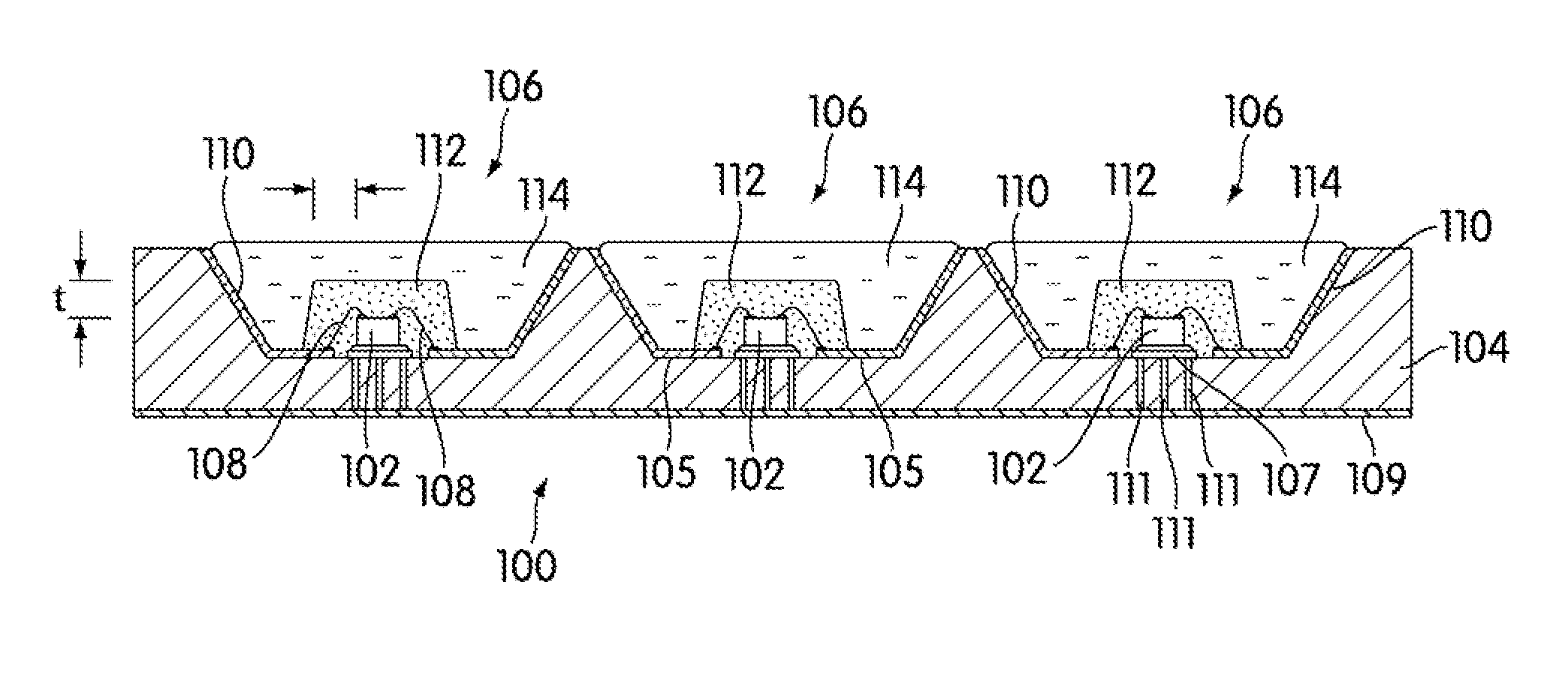
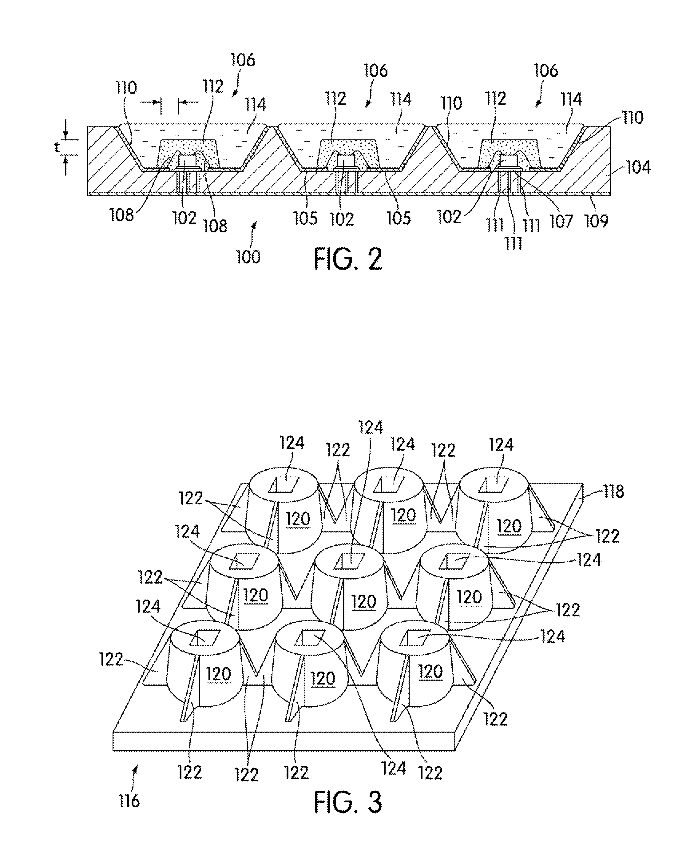
[0055]FIG. 2 is a schematic sectional view of a white light emitting device 100 in accordance with a first embodiment of the invention. The device 100 comprises an array of blue (i.e. dominant wavelength in a range ≈400 to 480 nm) surface emitting InGaN / GaN (indium gallium nitride / gallium nitride) based light emitting diode (LED) chips 102 packaged in a high temperature package 104 such as for example a low temperature co-fired ceramic (LTCC) package of a type as described in co-pending U.S. Patent Application Publication No. 2009 / 0294780 A1 (Ser. No. 12 / 127,749 filed May 27, 2008) the specification and drawings of which are incorporated herein by reference. In FIG. 2 the device 100 comprises a square array of nine LED chips 102 (3 rows by 3 columns), though it will be appreciated that the device of the invention applies to other LED chip configurations that can comprise many more LED chips. The package 104 has in an upper surface a square array of circular recesses (c...

2nd embodiment

2nd Embodiment

[0078]FIG. 6 is a schematic sectional representation of a light emitting device 100 in accordance with a second embodiment of the invention. In this embodiment an array of blue (i.e. wavelength≈400 to 480 nm) surface emitting InGaN / GaN (indium gallium nitride / gallium nitride) based light emitting diode (LED) chips 102 is mounted on a substantially planar substrate 142 such as for example a metal core printed circuit board (MCPCB)—a so called chip on board (COB) arrangement. As is known MCPCBs are commonly used for mounting electrical components that generate large amounts of heat and comprise a layered structure comprising a thermally conducting base 144, typically a metal such as aluminum (Al), and alternating layers of an electrically non-conducting / thermally conducting dielectric material 146 and electrically conducting tracks 148, typically made of copper (Cu). The dielectric layers 146 are very thin such that they can conduct heat from components mounted on the el...

3rd embodiment

3rd Embodiment

[0091]FIG. 8 is a schematic sectional representation of a light emitting device 100 in accordance with a third embodiment of the invention. In this embodiment an array of surface emitting InGaN / GaN based light emitting diode (LED) chips 102 are mounted on a planar substrate 142 such as for example a printed circuit board, MCPCB or ceramic circuit board. Each LED chip 102 is encapsulated with a phosphor coating 112 that is substantially conformal in form and the phosphor coating is itself encapsulated within a light transmissive (transparent) cover 162 that provides environmental protection of the phosphor encapsulation 112. The transparent cover 162 further defines a respective lens element 164 corresponding to each LED chip 102 for focusing or otherwise directing light emission from the device. As will be described the transparent cover 162 is used to mold the phosphor encapsulation 112 and is left in situ. Due to the dual function of the cover 162, that is as both a ...


PUM


Abstract

A light emitting device comprises: a package (low temperature co-fired ceramic) having a plurality of recesses (cups) in which each recess houses at least one LED chip and at least one phosphor material applied as coating to the light emitting light surface of the LED chips, wherein the phosphor material coating is conformal in form. In another arrangement a light emitting device comprises: a planar substrate (metal core printed circuit board); a plurality of light emitting diode chips mounted on, and electrically connected to, the substrate; a conformal coating of at least one phosphor material on each light emitting diode chip; and a lens formed over each light emitting diode chip.

Description

CROSS-REFERENCE TO RELATED APPLICATIONS[0001]This application claims the benefit of priority to U.S. Provisional Application No. 61 / 146,379, filed Jan. 22, 2009, entitled “Light Emitting Device with Phosphor Wavelength Conversion and Methods of Manufacture Thereof” by Yi-Qun Li et al, the specification and drawings of which are incorporated herein by reference.BACKGROUND OF THE INVENTION[0002]1. Field of the Invention[0003]The invention relates to light emitting devices with phosphor wavelength conversion and to methods of applying one or more phosphor materials to a light emitting diode (LED) chip. More particularly, although not exclusively, the invention concerns light emitting devices in which the one or more phosphor materials comprise a conformal coating.[0004]2. Description of the Related Art[0005]White light emitting LEDs (“white LEDs”) are known in the art and are a relatively recent innovation. It was not until LEDs emitting in the blue / ultraviolet part of the electromagne...

Claims


Application Information

Patent Timeline
IPC IPC(8): H01L33/00
CPCH01L33/44H01L33/501H01L33/54H01L2933/0041H01L2933/005H01L2224/73265H01L2224/48091H01L2924/00014
Inventor LI, YI-QUNMELMAN, JONATHANCOLLIER, IAN
Owner INTEMATIX
Why Eureka
Try Eureka