Manufacturing method of a boride film, and manufacturing method of an electron-emitting device

Inactive Publication Date: 2010-07-29
CANON KK
View PDF5 Cites 7 Cited by
  • Summary
  • Abstract
  • Description
  • Claims
  • Application Information

AI Technical Summary

Benefits of technology

[0005]In producing an electron-emitting device using a lanthanum boride film, it is preferable, from the viewpoint of the stability of electron emission, etc., that the film has higher crystallinity. In addition, in the orientation of crystals, an orie

Problems solved by technology

When a position dependency of film quality was large at this time, it was difficult t

Method used


Image

  • Manufacturing method of a boride film, and manufacturing method of an electron-emitting device
  • Manufacturing method of a boride film, and manufacturing method of an electron-emitting device
  • Manufacturing method of a boride film, and manufacturing method of an electron-emitting device

Examples


Example

First Example

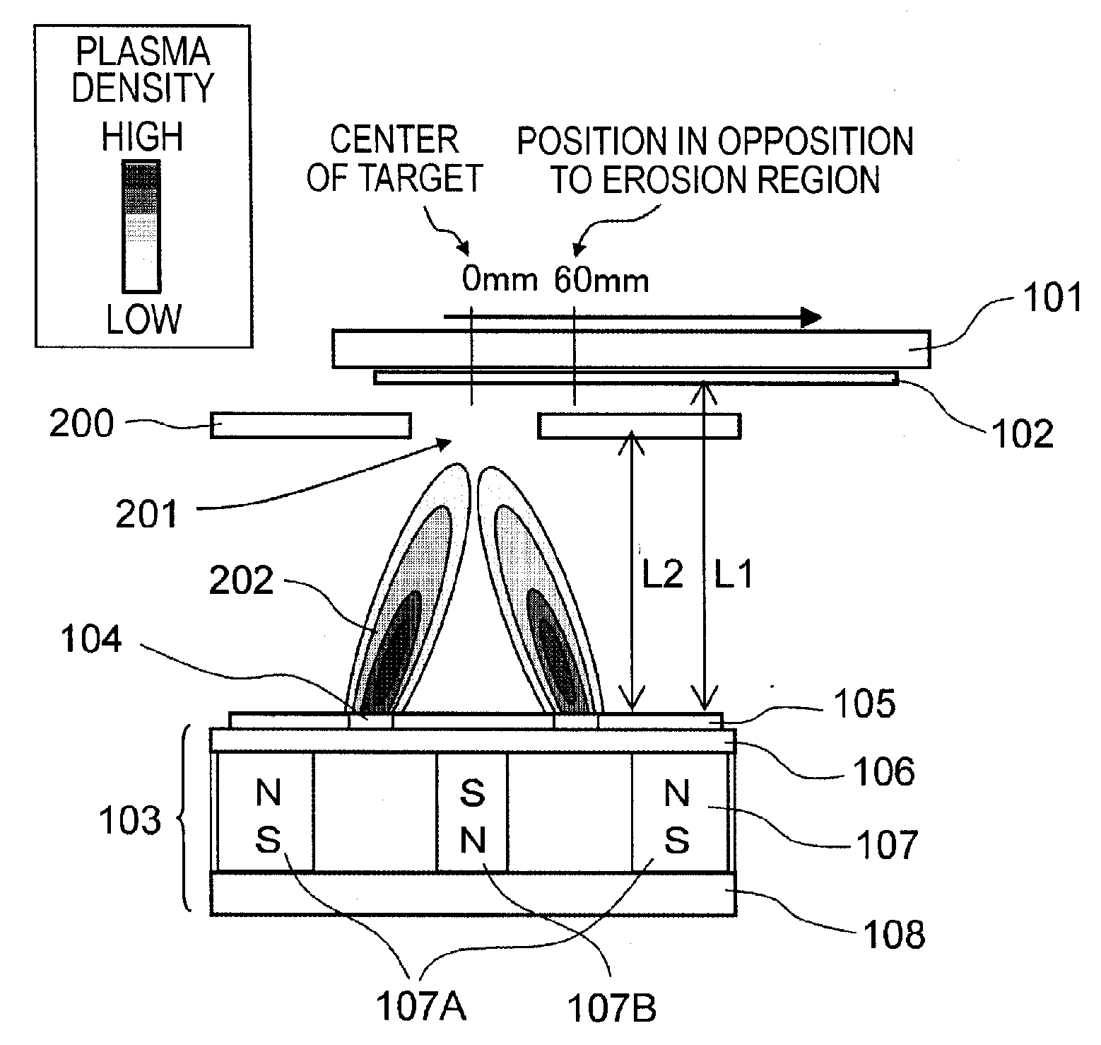
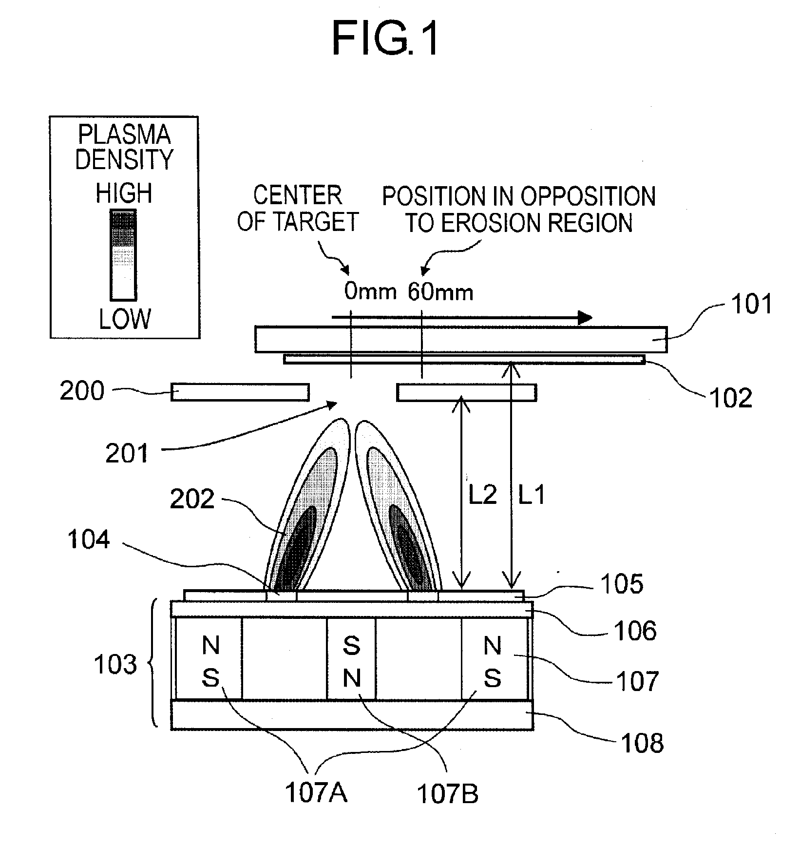
[0053]A lanthanum hexaboride target 105 of a circular shape having a diameter of 8 inches and a Si-wafer substrate 102 were used, and the substrate 102 and the target 105 were arranged in opposition to each other, as shown in FIG. 1. An erosion region 104 was formed at a position spaced by a distance of 60 mm from the center of the target. A shield plate 200 is arranged vertically above the target 105, and a mask of an entire erosion opposed region of the substrate 102 was masked. In addition, the shield plate 200 has an opening portion 201 arranged above the central portion of the target 105. A distance L1 between the substrate 102 and the target 105 was set to 90 mm, and a distance L2 between the shield plate 200 and the target 105 was set to 70 mm. The degree of vacuum at the time of exhausting under high vacuum was set to 2×10⁻⁴ Pa.

[0054]By using a convergence type magnet having a magnetic field of 1,000 G as a magnet 107, a plasma density distribution 202 was forme...

Example

First Comparative Example

[0055]A lanthanum boride film of a first comparative example was formed by means of the same method as the first example except for using a divergence type magnet having a magnetic field 1,000 G instead of the convergence type magnet. In the first comparative example, a plasma density in an opening portion 201 was lower than that in its peripheral region.

[0056]The lanthanum boride films obtained according to the first example and the first comparative example were individually analyzed by means of an X-ray diffraction method. For the film of the first example, the FWHM of a diffraction peak on a (100) surface was 0.55 degrees, and a value obtained by dividing the integral value of the diffraction peak on the (100) surface by the integral value of a diffraction peak of a (110) surface was 3.3. On the other hand, for the film of the first comparative example, the FWHM of a diffraction peak on a (100) surface was 0.80 degrees, and a value obtained by dividing t...

Example

Second Example

[0057]A manufacturing method of an electron-emitting device according to a second example will be described with reference to FIG. 4A-FIG. 4F. FIG. 4A-FIG. 4F are diagrammatic illustrations sequentially showing the manufacturing steps of the electron-emitting device.

[0058]A substrate 401 is a substrate for supporting an element in a mechanical manner. In this example, a PD 200, which is a low sodium glass developed for plasma displays, was used as the substrate 401.

[0059]First, as shown in FIG. 4A, insulating layers 403, 404 and a conductive layer 405 were laminated on the substrate 401. The insulating layers 403, 404 are insulating films, respectively, which are made of materials which are excellent in processability. In the second example, the insulating layer 403 of silicon nitride (SixNy) having of a film thickness 500 nm and the insulating layer 404 of silicon oxide (SiO2) having a film thickness of 30 nm were formed by means of a sputtering method. In addition, t...


PUM

PropertyMeasurementUnit
Densityaaaaaaaaaa
Magnetic flux densityaaaaaaaaaa
Erosion-corrosion rateaaaaaaaaaa

Abstract

A boride film is deposited on a substrate through an opening portion a shield member located between the substrate and a target by means of a sputtering method. The shield member is arranged so as to shield between an erosion region of the target and the substrate. A distribution of plasma density in a space between the substrate and the target is set in such a manner that a plasma density in a region in which the opening portion is located becomes higher than a plasma density in a region shielded by the shield member.

Description

BACKGROUND OF THE INVENTION[0001]1. Field of the Invention[0002]The present invention relates to a production method of a boride film using a sputtering method, and a production method of an electron-emitting device.[0003]2. Description of the Related Art[0004]A field emission type electron-emitting device is an electron-emitting device of the type that applies a voltage (electric field) across a cathode electrode (and an electron emission structure arranged thereon) and a gate electrode, and pulls out electrons into a vacuum from a cathode electrode side by means of this voltage (electric field). Therefore, the operating electric field is greatly influenced by the work function, shape, etc., of the cathode electrode (electron emission structure) to be used. Theoretically, it is considered that the smaller the work function of the cathode electrode (electron emission film), with the lower operating voltage the cathode electrode can be driven. In Japanese patent application laid-open...

Claims


Application Information

Patent Timeline
IPC IPC(8): C23C14/46
CPCC23C14/067C23C14/54C23C14/35C23C14/225
Inventor AOKI, NAOFUMIMIZUNO, TOMOYASUKOBAYASHI, TAMAKIMIYAMOTO, YUSUKE
Owner CANON KK
Why Eureka
Try Eureka