Semiconductor laser device

a laser device and semiconductor technology, applied in semiconductor lasers, laser details, electrical devices, etc., can solve the problems of small light contribution to the oscillation of a te mode, and the efficiency of the laser oscillation is not necessarily excellent, and achieve the effect of reducing the threshold current and superior energy efficiency

Inactive Publication Date: 2010-08-05
ROHM CO LTD
View PDF10 Cites 251 Cited by
  • Summary
  • Abstract
  • Description
  • Claims
  • Application Information

AI Technical Summary

Benefits of technology

[0007]One of the important characteristics of a semiconductor laser diode is a threshold current (an oscillation threshold) for

Problems solved by technology

However, light emitted from an active layer grown on a major surface defined by a c-plane is randomly polarized, and hence the ratio of light contributing to oscillation of a TE mode is

Method used


Image

  • Semiconductor laser device
  • Semiconductor laser device
  • Semiconductor laser device

Examples


Embodiment Construction

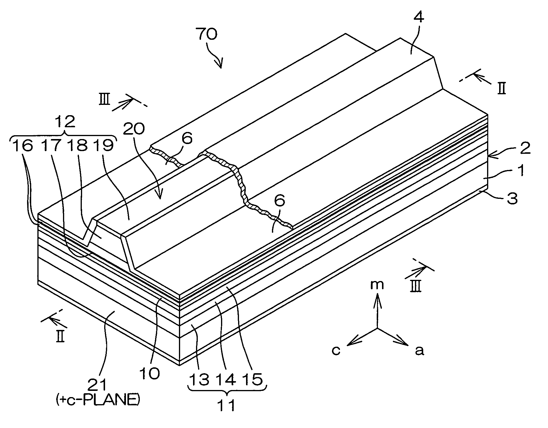
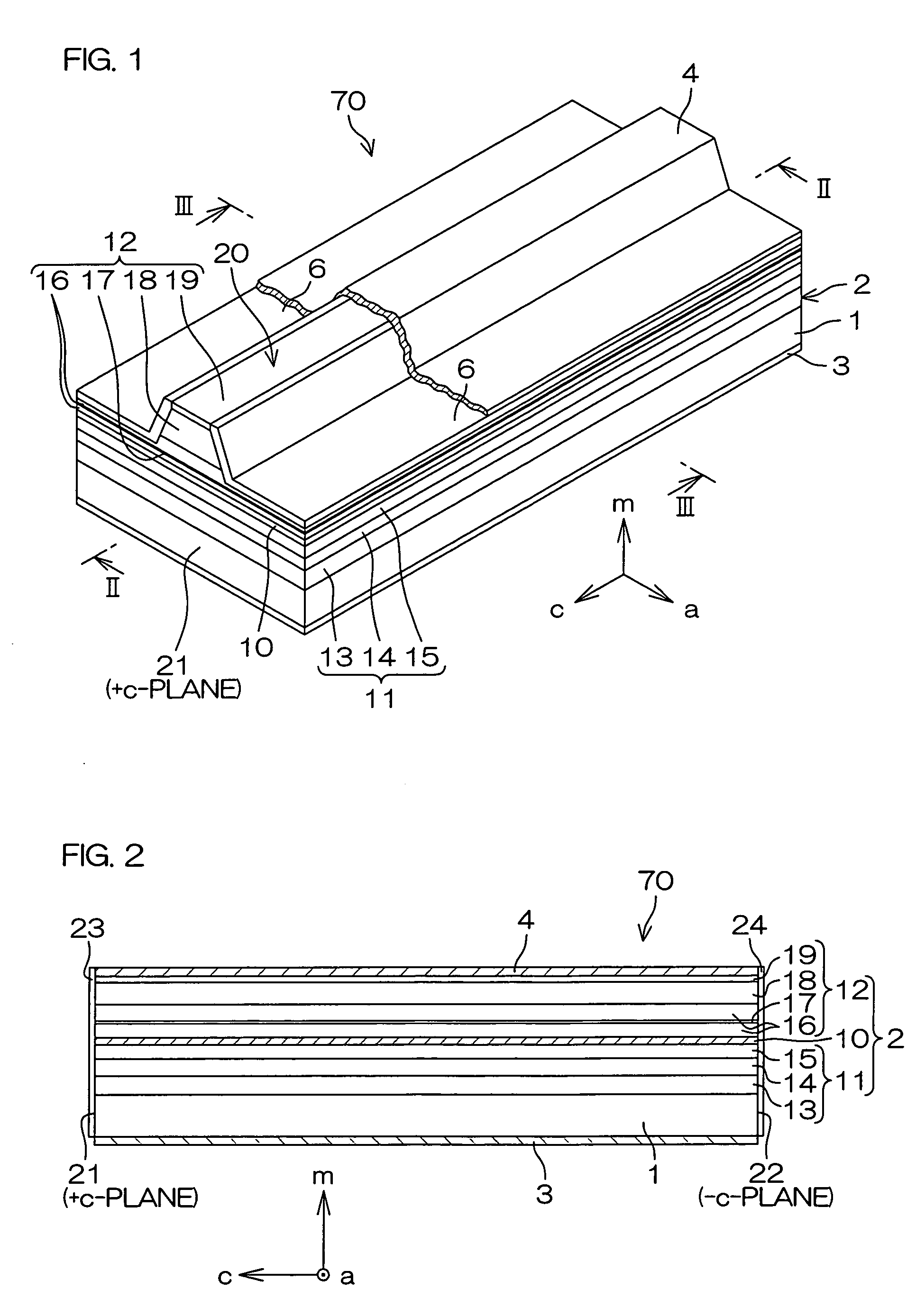
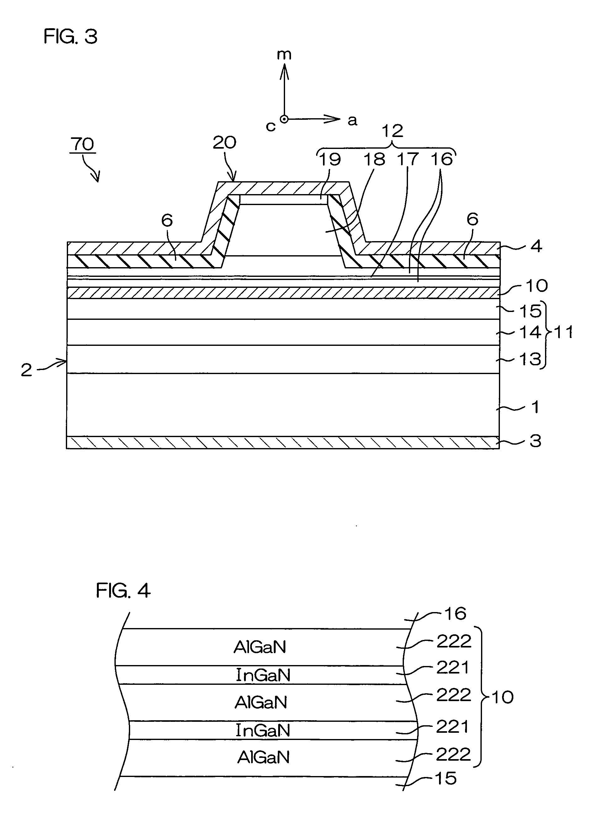
[0031]An embodiment of the present invention provides a semiconductor laser device having a semiconductor laser diode structure made of group III nitride semiconductors having major growth surfaces defined by nonpolar planes or semipolar planes. The semiconductor laser diode structure includes a p-type cladding layer and an n-type cladding layer, a p-type guide layer and an n-type guide layer held between the p-type cladding layer and the n-type cladding layer, and an active layer containing In held between the p-type guide layer and the n-type guide layer. The In compositions in the p-type guide layer and the n-type guide layer are increased as approaching the active layer respectively.

[0032]According to the structure, the In compositions in the guide layers are increased as approaching the active layer (a light emitting layer), whereby an excellent light confining effect can be attained. In other words, the thicknesses of the guide layers may not be increased, or the total In comp...


PUM


Abstract

A semiconductor laser device has a semiconductor laser diode structure made of group III nitride semiconductors having major growth surfaces defined by nonpolar planes or semipolar planes. The semiconductor laser diode structure includes a p-type cladding layer and an n-type cladding layer, a p-type guide layer and an n-type guide layer held between the p-type cladding layer and the n-type cladding layer, and an active layer containing In held between the p-type guide layer and the n-type guide layer. The In compositions in the p-type guide layer and the n-type guide layer are increased as approaching the active layer respectively. Each of the p-type guide layer and the n-type guide layer may have a plurality of InxGa1-xN layers (0≦x≦1). In this case, the plurality of InxGa1-xN layers may be stacked in such order that the In compositions therein are increased as approaching the active layer.

Description

BACKGROUND OF THE INVENTION[0001]1. Field of the Invention[0002]The present invention relates to a semiconductor laser device having a semiconductor laser diode structure made of group III nitride semiconductors.[0003]2. Description of Related Art[0004]Group III nitride semiconductors are group III-V semiconductors employing nitrogen as a group V element, and typical examples thereof include aluminum nitride (AlN), gallium nitride (GaN) and indium nitride (InN). The group III nitride semiconductors can be generally expressed as AlXInYGa1-X-YN (0≦X≦1, 0≦Y≦1 and 0≦X+Y≦1).[0005]A violet short-wavelength laser source is increasingly used in the fields of high-density recording in an optical disk represented by a DVD, image processing, medical equipment, measuring equipment and the like. Such a short-wavelength laser source is constituted of a laser diode employing GaN semiconductors, for example.[0006]A GaN semiconductor laser diode is manufactured by growing group III nitride semicondu...

Claims


Application Information

Patent Timeline
IPC IPC(8): H01S5/34H01S5/323
CPCB82Y20/00H01S5/2004H01S5/34333H01S5/2205H01S5/3202H01S5/2201H01S5/2009H01S5/2031H01S5/3213H01S5/32025
Inventor OKAMOTO, KUNIYOSHIKUBOTA, MASASHITANAKA, TAKETOSHIKASHIWAGI, JUNICHITANAKA, YOSHINORI
Owner ROHM CO LTD
Why Eureka
Try Eureka