Dry etching method for silicon nitride film
- Summary
- Abstract
- Description
- Claims
- Application Information
AI Technical Summary
Benefits of technology
Problems solved by technology
Method used
Image

Examples
first embodiment
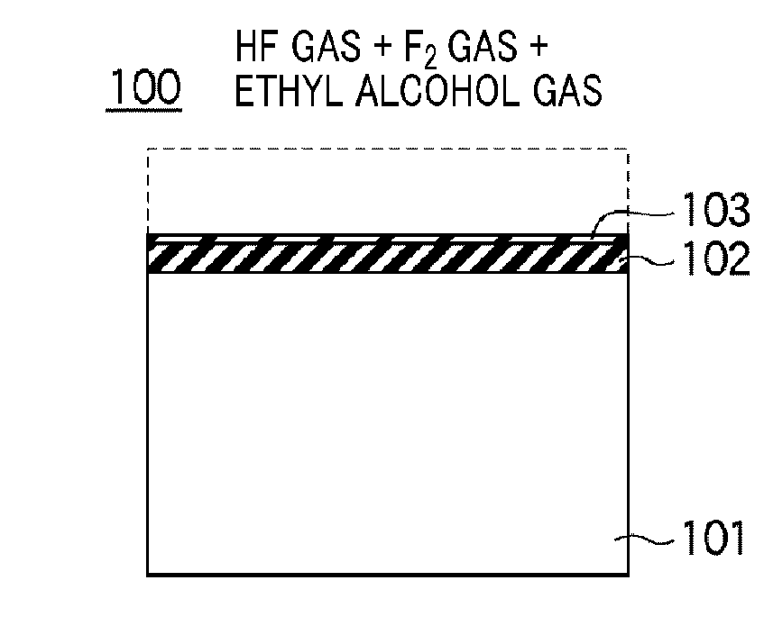
[0038]A first embodiment is described for the case of dry-etching a silicon nitride film formed on a semiconductor wafer (hereinafter, simply referred to as a wafer) as an example processing target object.
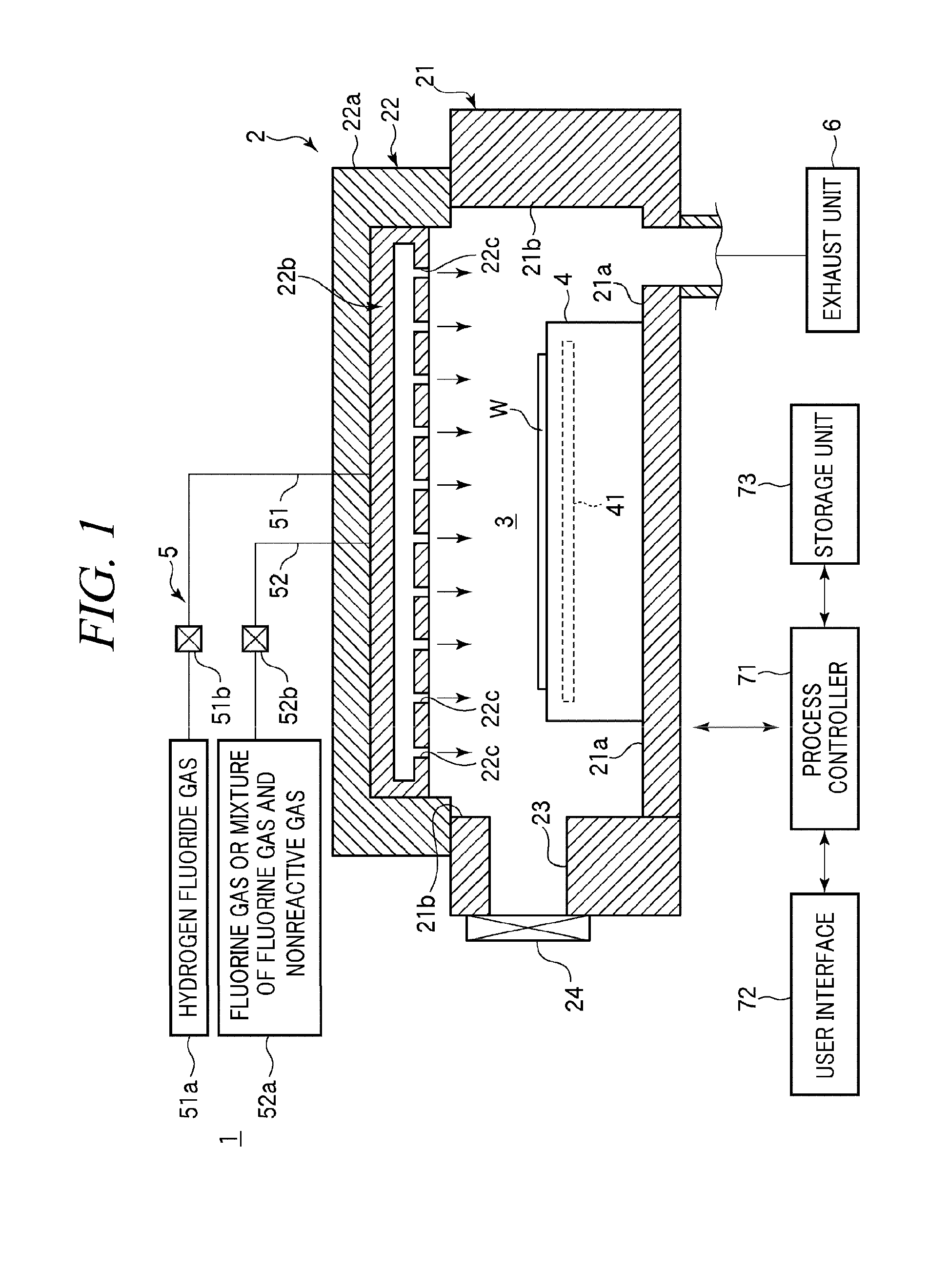
[0039]FIG. 1 is a cross sectional view schematically showing an example dry etching apparatus used in the dry etching method for the silicon nitride film in accordance with the first embodiment of the present disclosure.
[0040]As illustrated in FIG. 1, a dry etching apparatus 1 includes a hermetically sealed chamber 2. The inside of the chamber 2 is configured as a processing space 3 in which a wafer W as the example processing target object is accommodated. A stage 4 configured to mount the wafer W in a substantially horizontal manner is installed within the chamber 2. A gas supply unit 5 that supplies a processing gas into the chamber 2 and an exhaust unit 6 that evacuates the chamber 2 are installed outside the chamber 2.
[0041]In the present embodiment, the chamber 2 includes a c...
second embodiment
[0072]A silicon nitride film (e.g., LP—SiN) is dry-etched using a processing gas containing at least a hydrogen fluoride gas and a fluorine gas when a base is silicon (silicon wafer) and a silicon oxide film (e.g., a thermal oxide film (Th-Ox)) is used as an etching stopper.
[0073]Further, overetching is performed to completely remove the silicon nitride film from the entire surface of the silicon wafer.
[0074]However, the base silicon was observed to be roughened when the silicon nitride film was over-etched. The present inventors have conjectured the reason for the roughness as follows.
[0075]The silicon nitride film does not only contain silicon and nitrogen but it also contains a very small amount of oxygen as well. The very small amount of oxygen forms SiO2 locally in the silicon nitride film. If the silicon nitride film having the locally-formed SiO2 is etched using the processing gas containing at least the hydrogen fluoride gas and the fluorine gas, water (H2O) is generated, as...
first example
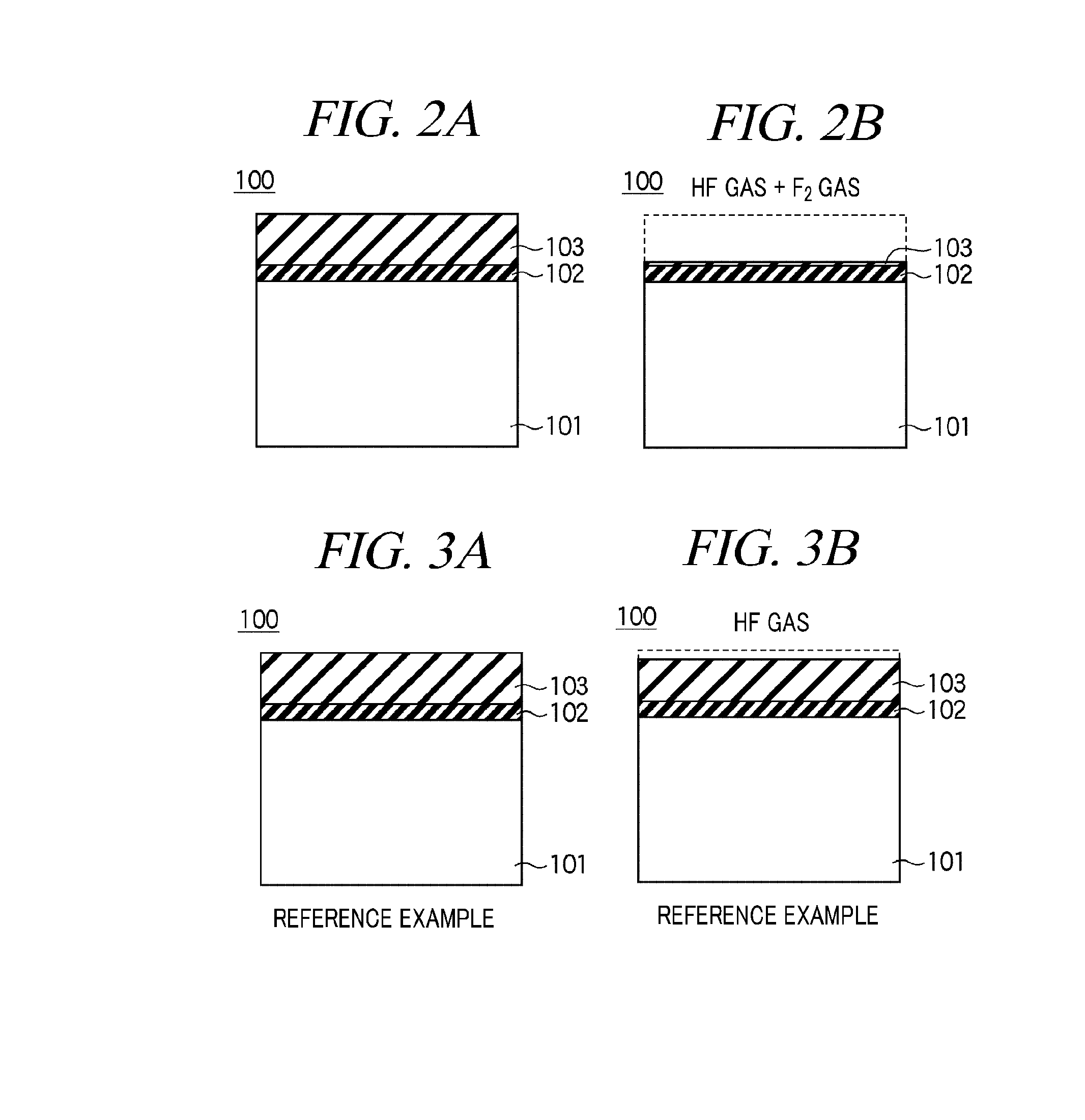
[0081]FIGS. 7A and 7B are cross sectional views illustrating a first example of the dry etching method in accordance with the second embodiment of the present disclosure.
[0082]As illustrated in FIG. 7A, in the first example, dry etching is performed using a processing gas containing at least a hydrogen fluoride gas and a fluorine gas until just-etching or almost just-etching of the silicon nitride film 103 is achieved. Example conditions for this dry etching process are as follows. An internal pressure of the processing space 3 is about 50 Torr; a flow rate ratio (HF / X) between the hydrogen fluoride gas and the gas mixture (X) is about 1500 sccm / 1500 sccm; a stage temperature is about 150° C.; and an etching time is about 140 seconds.
[0083]Then, subsequent overetching is performed by dry etching using only a HF gas, as shown in FIG. 7B. Example dry etching conditions for the overetching are as follows. The hydrogen fluoride gas (HF) is about 1500 sccm; a stage temperature is about 1...
PUM
 Abstract
Description
Claims
Application Information
 - R&D
- Intellectual Property
- Life Sciences
- Materials
- Tech Scout
- Unparalleled Data Quality
- Higher Quality Content
- 60% Fewer Hallucinations
Browse by: Latest US Patents, China's latest patents, Technical Efficacy Thesaurus, Application Domain, Technology Topic, Popular Technical Reports.
© 2025 PatSnap. All rights reserved.Legal|Privacy policy|Modern Slavery Act Transparency Statement|Sitemap|About US| Contact US: help@patsnap.com