Dual sided processing and devices based on freestanding nitride and zinc oxide films

Inactive Publication Date: 2010-08-12
GOLDENEYE
View PDF11 Cites 39 Cited by
  • Summary
  • Abstract
  • Description
  • Claims
  • Application Information

AI Technical Summary

Benefits of technology

[0032]As current density increases on devices like LEDs, current spreading becomes a limiting factor in device performance especially for large area devices. In co-pending patent applications, freestanding nitride films on which MQWs are grown can be stacked and interconnected. By using the highly transparent conductive layers described herein, emitting volumes can be formed. Rather than have a very large die with large variations in drive currents across the die, stacked die can not only improve the current spreading across a given area but increase the lumens/etendue or radiance of the device. Similarly, this same technique can be use to form more efficient and concentrated solar cells and electronic devices such as IGFETS. With nitrides, current spreading limitations tend to be more severe than thermal effects, therefore volume emitters tend to be more efficient than surface emitters. Low absorption and high quality ohmic contacts are required to enable volume emitters like these. The use of epitaxially grown transparent conductive layers on freestanding nitride films stacked to form volume emitters, absorbers, and electrical devices is an embodiment of this invention.
[0033]Geometry plays a critical role in volume emitters versus surface emitters. Here is a simple example: A typical nitride LED less than 10 microns in thickness and 300 micron×300 micron in area has an emitting area equal to 0.09 mm2. If the same size die is 100 micron thick there is more emitting area, 0.12 mm2, on the sides of the die than the top surface. There are a number of advantages to this configuration. It is well known that recombination losses are minimized directly under electrical contacts on LEDs. Utilizing large reflective contacts on the top and bottom of the freestanding nitride LED enable very high extraction efficiency out the sides of the die This extraction efficiency is further enhanced by the tendency for a substantial portion of the light generated within the active layer to be waveguided to the edges. The use of thick freestanding nitride films to create LEDs in which the output area of the surface normal to the active layer plane is larger than the

Problems solved by technology

Silicon has been used as the substrate material of choice due to cost and availability of single crystal silicon wafers.
However, heretofore there has not been an economical solution to using these materials without growing them or attaching them to secondary substrates.
Silicon also has limitations with regard to operating temperature as well as other critical material parameters; this limits silicon's usefulness in optical, power and high-frequency applications.
Unfortunately, nitrides are not available in wafer form at a reasonable price or reasonable quality.
Even if such wafers were to become available, costly growth, dicing, and thinning techniques would be required to create useful devices.
While native ZnO wafers have been fabricated, their cost is restrictive and they lack a suitable/stable p-dopant which limit their applications.
In some cases, processing round wafers is actually a disadvantage or limitation to be overcome.
Also the resulting structure suffers from poor thermal performance, thermal expansion mismatch which limits operating range.
This is due to the fragile nature of the thin nitride film

Method used


Image

  • Dual sided processing and devices based on freestanding nitride and zinc oxide films
  • Dual sided processing and devices based on freestanding nitride and zinc oxide films
  • Dual sided processing and devices based on freestanding nitride and zinc oxide films

Examples


Embodiment Construction

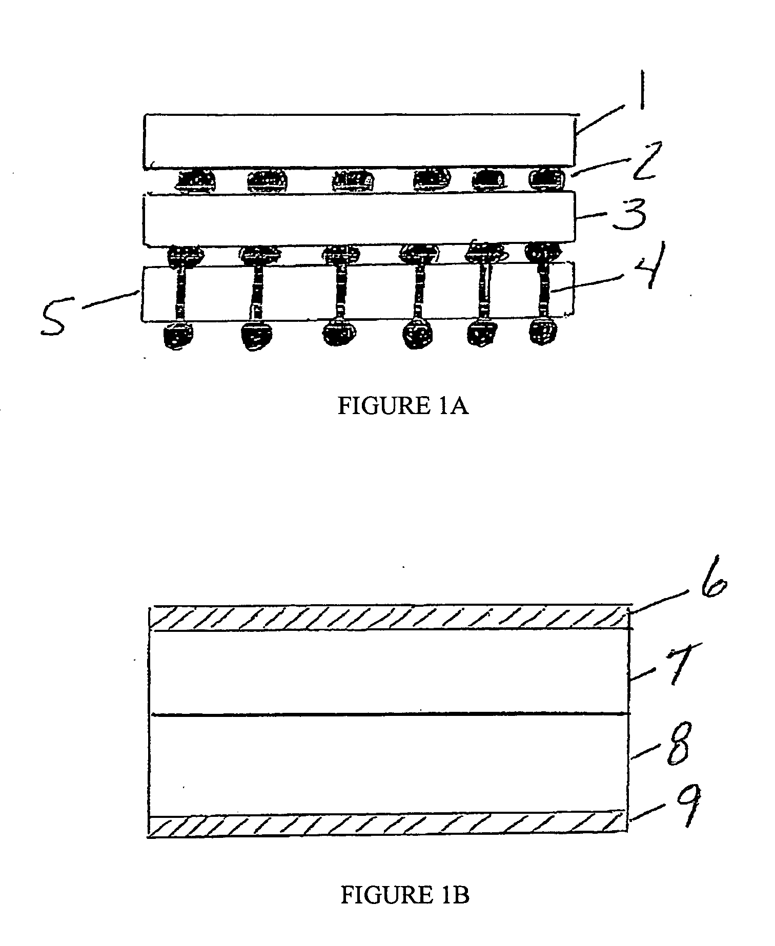
[0055]FIG. 1A depicts a typical prior art three-dimensional device based on stacked silicon chips. Thinning is used to reduce the device thickness for both via formation, overall device thickness and thermal performance. This technique is used especially for memory devices to increase the amount of memory that can be contained within a given footprint. Memory layers 1, 3, and 5 are typically freestanding silicon films which are physically and electrically connected via interconnects 2. In this case, a via 4 may be used through the freestanding silicon films such that a high level of interconnect is created. However, the thinning processes used (polishing, etching, etc) negatively impact overall process yield and ultimate device cost.

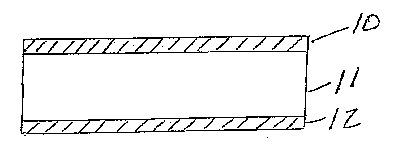
[0056]FIG. 1B depicts a prior art technique to form a large area diode by using n doped layer 7 and p doped layer 8 with contacts 6 and 9. The resulting PN junction can be formed by growing n doped layer 7 or p doped layer 8 on the other layer or may be ...


PUM


Abstract

Thin freestanding nitride films are used as a growth substrate to enhance the optical, electrical, mechanical and mobility of nitride based devices and to enable the use of thick transparent conductive oxides. Optoelectronic devices such as LEDs, laser diodes, solar cells, biomedical devices, thermoelectrics, and other optoelectronic devices may be fabricated on the freestanding nitride films. The refractive index of the freestanding nitride films can be controlled via alloy composition. Light guiding or light extraction optical elements may be formed based on freestanding nitride films with or without layers. Dual sided processing is enabled by use of these freestanding nitride films. This enables more efficient output for light emitting devices and more efficient energy conversion for solar cells.

Description

REFERENCE TO PRIOR APPLICATION[0001]This application claims the benefit of U.S. Provisional Patent Application Ser. No. 61 / 198,484, which was filed on Nov. 5, 2008, which is herein incorporated by reference.BACKGROUND OF THE INVENTION[0002]Semiconductor devices are used in a wide variety of applications. Silicon has been used as the substrate material of choice due to cost and availability of single crystal silicon wafers. Driven by the microelectronic industry silicon wafer production has enabled the economical use of larger wafers with greater than 12 inch diameter. The low cost of silicon allows thick (1-2 mm) single crystal silicon wafers to be used without a secondary substrate for handling and processing. This enables the formation of large area die, which can be processed without the need for transfer substrates or wafer bonding. Additionally, the properties of silicon permit wafers to be doped so that 3 dimensional devices (via planar processing) can be created taking advant...

Claims


Application Information

Patent Timeline
IPC IPC(8): H01L33/04H01L29/66H01L21/20
CPCH01L21/02389H01L21/02403H01L21/02521H01L21/0254H01L2924/1461H01L33/0075H01L2224/13H01L31/06H01L2924/00
Inventor ZIMMERMAN, SCOTT M.BEESON, KARL W.LIVESAY, WILLIAM R.
Owner GOLDENEYE
Why Eureka
Try Eureka