Method for producing semiconductor device and semiconductor device produced by same method

Inactive Publication Date: 2010-08-19
SHARP KK
View PDF22 Cites 8 Cited by
  • Summary
  • Abstract
  • Description
  • Claims
  • Application Information

AI Technical Summary

Benefits of technology

[0183]A bubble appears to form as follows. Namely, in response to the heat treatment, H2, H2O, and the like, which exist in the interface or in the film, move toward and concentrate in a region in which the binding energy is weak. This will cause the bubbles to be formed. It appears that, if the heat treatment is continued even after the peeled layer is peeled, during such a heat treatment, H2, H2O, and the like (i) move toward and concentrate in the interface region in which the binding energy is weak, and then (ii) expand in volume, so that bubbles are formed. In view of the circumstances, it appears to be possible to prevent such bubbles from occurring by ending the heat treatment immediately after the peeled layer is peeled. Actually, the inventors of the present invention conducted a study on whether or not the number of generated bubbles increased in a case where the heat treatment was continued after the peeled layer was peeled. Specifically, the inventors of the present invention carried out the heat treatment with respect to the glass substrate at 580° C., carried out an additional heat treatment with respect to the glass substrate at 600° C., and then counted with a microscope the number of bubbles caused. The result is shown in FIG. 6.
[0184]FIG. 6 clearly shows that such an additional heat treatment caused bubbles to form. It appears that the reason why the bu

Problems solved by technology

The occurrence of any of such localized energy levels has caused problems such as a decrease in mobility and/or an increase in subthreshold coefficient (S coefficient) in transistors.
This ultimately caused a degradation in performance of the transistors.
Further, in a case where the silicon film of a polysilicon film has defective crystallinity, fixed electric charge were easily generated in an interface between the silicon film and a gate insulating film in a thin film transistor.
This generation of such fixed electric charge made it difficult to control a threshold voltage of the thin film transistor, and made it difficult to ach

Method used


Image

  • Method for producing semiconductor device and semiconductor device produced by same method
  • Method for producing semiconductor device and semiconductor device produced by same method
  • Method for producing semiconductor device and semiconductor device produced by same method

Examples


Example

Example 1

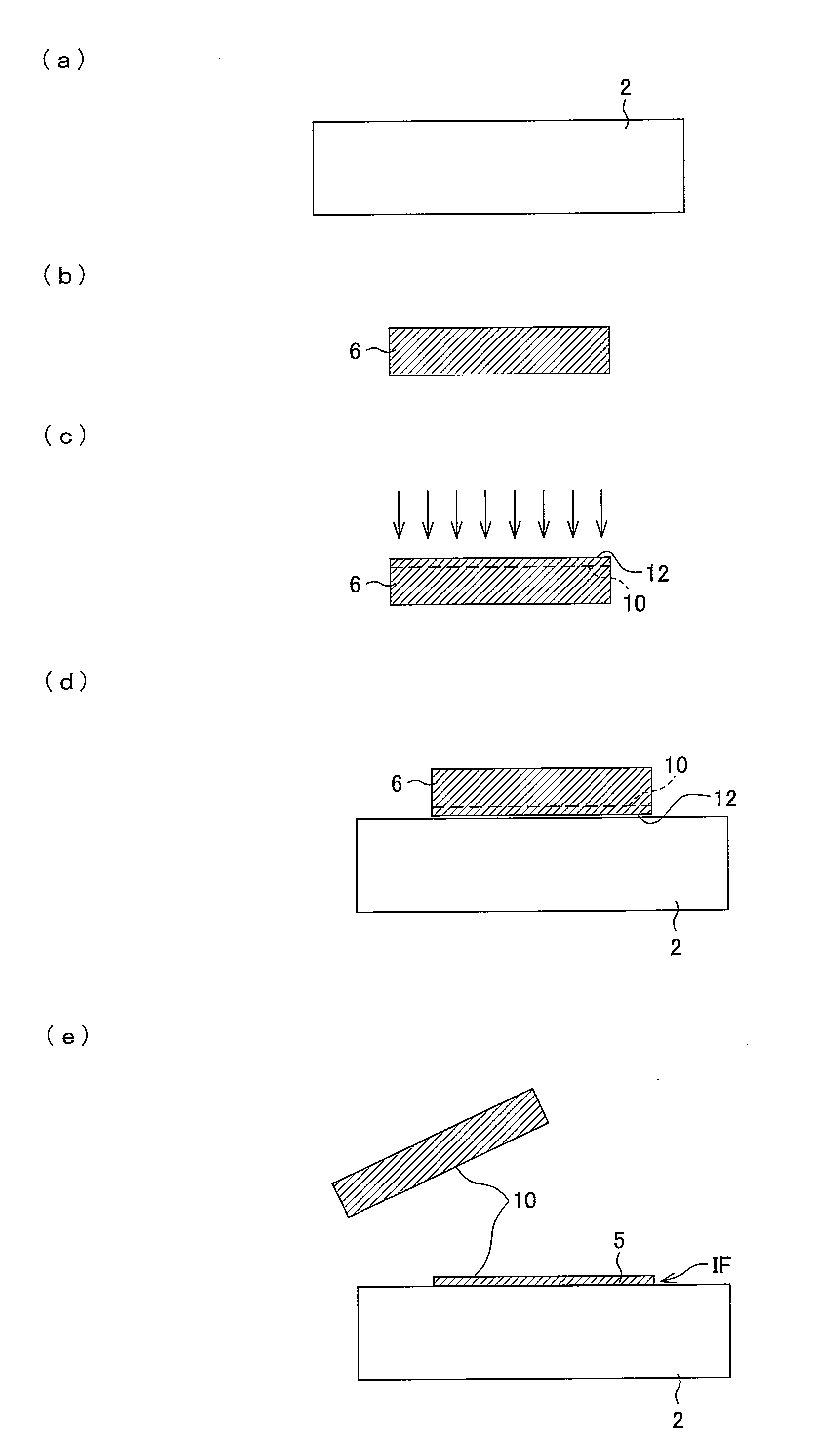
[0187]A device in which a peeled layer was formed by implanting hydrogen into a single-crystal Si substrate was prepared. Next, a SiO2 film was formed on a surface of the device. The SiO2 film was planarized by CMP. Note that the hydrogen was implanted under the condition that implanting energy is 150 keV and an implanting rate is 6 E 16 cm−2.

[0188]The device, having the SiO2 film on its surface, was heated in vacuum at 350° C. for 2 hours so as to cause gases such as H2 and H2O to escape from the film. The device was cut, by a method such as the dicing, so as to have a desired size, and is then subjected to a surface treatment (SC1 treatment) so as to have hydrophilicity.

[0189]A similar surface treatment was carried out with respect to a glass substrate, onto which the device was to be transferred. After that, the transferring was carried out by directly combining the device with a surface of the glass substrate.

[0190]A part of the device was peeled under the condition tha...

Example

Example 2

[0192]A peeled layer was formed by thermally oxidizing a single-crystal Si substrate, and then by implanting hydrogen into the single-crystal Si substrate. A surface treatment (SC1 treatment) was carried out with respect to the single-crystal Si substrate and a glass substrate onto which the single-crystal Si substrate was to be transferred. Then, the single-crystal Si substrate was transferred onto the glass substrate by combining the substrates with each other. Note that the glass substrate can be cut so as to have a desired size.

[0193]The device prepared by the above method had a bubble density of not more than five bubbles / cm2.

Example

Example 3

[0194]A device in which a peeled layer was formed by implanting H or hydrogen into a single-crystal Si substrate was prepared. Next, a SiO2 film was formed on a surface of the device. The SiO2 film was planarized by CMP. Note that the hydrogen was implanted under the condition that implanting energy is 130 keV and an implanting rate is 4 E 16 cm−2.

[0195]The device was cut by the dicing so as to have a desired size. Then, a surface treatment was carried out with respect to a glass substrate onto which the device was to be transferred. After that, the transferring was carried out by combining the device with the glass substrate.

[0196]A part of the device was peeled under the condition that a temperature-raising rate was 5° C. / min and a heating temperature was within a range from 550° C. to 700° C. The heat treatment increases a binding energy in the interface. After the part of the device was peeled, (i) the heat treatment was ended immediately and (ii) the part thus peeled w...


PUM


Abstract

To prevent bubbles from occurring along a transfer interface, the present method includes the steps of: forming a peeled layer 10 in a transferred member 6 by implanting a peeled-layer forming substance into the transferred member 6; forming a planar surface in the transferred member 6 by planarizing a surface of the transferred member 6; forming a composite including the transferred member 6 and a glass substrate 2 by directly combining the transferred member 6 via the planar surface with a surface of the glass substrate 2; and peeling a part of the transferred member 6 from the composite along the peeled layer 10 serving as an interface by heat-treating the composite.

Description

TECHNICAL FIELD[0001]The present invention relates to a method for producing a semiconductor device and to a semiconductor device produced by this method. The present invention particularly relates to (i) a method for forming, e.g., a single-crystal silicon film on a substrate such as a glass substrate by transferring, onto the substrate, a single-crystal chip of a semiconductor such as silicon, a semiconductor chip, and / or a semiconductor device, and to (ii) various devices produced by the method.BACKGROUND ART[0002]Conventionally, the following techniques (i) and (ii) have been proposed, and have greatly advanced interdependently on at least growth in use of liquid crystal displays: (i) an integrated circuit element technique in which a single-crystal silicon substrate is processed so that approximately hundreds of millions of transistors are formed on the single-crystal silicon substrate; and (ii) a thin film transistor (TFT) technique in which a polycrystalline semiconductor fil...

Claims


Application Information

Patent Timeline
IPC IPC(8): H01L29/786H01L21/762H01L29/30
CPCH01L21/76254H01L29/66772H01L27/1266H01L27/1214
Inventor TAKEI, MICHIKOMATSUMOTO, SHINFUKUSHIMA, YASUMORITAKAFUJI, YUTAKA
Owner SHARP KK
Why Eureka
Try Eureka