Multilayer wiring substrate and method for manufacturing the same

a wiring substrate and multi-layer technology, applied in the direction of printed circuit non-printed electric components association, serial/solid-state device details, borehole/well accessories, etc., can solve the problems of reducing the reliability of connection between the surface connection terminal and the ic chip, unsatisfactory yield of the multi-layer wiring substrate, etc., to achieve the effect of reducing the reliability of connection and deteriorating the shape of the surface connection terminal

Active Publication Date: 2010-08-19
NGK SPARK PLUG CO LTD
View PDF2 Cites 32 Cited by
  • Summary
  • Abstract
  • Description
  • Claims
  • Application Information

AI Technical Summary

Benefits of technology

[0007]However, when the copper foil layer is removed through etching in the above-described conventional production process, etchant may invade into the interior of the laminated structure via the interfaces between the surface connection terminals and the resin insulating layers. In such a case, the copper layer of each surface connection terminal is likely to be etched out, which raises a problem of unsatisfactory yield of the multilayer wiring substrate. The deteriorated shape of the surface connection terminals caused by the etching out may lower the reliability of connection between the surface connection terminals and an IC chip.

Problems solved by technology

However, when the copper foil layer is removed through etching in the above-described conventional production process, etchant may invade into the interior of the laminated structure via the interfaces between the surface connection terminals and the resin insulating layers.
In such a case, the copper layer of each surface connection terminal is likely to be etched out, which raises a problem of unsatisfactory yield of the multilayer wiring substrate.
The deteriorated shape of the surface connection terminals caused by the etching out may lower the reliability of connection between the surface connection terminals and an IC chip.

Method used


Image

  • Multilayer wiring substrate and method for manufacturing the same
  • Multilayer wiring substrate and method for manufacturing the same
  • Multilayer wiring substrate and method for manufacturing the same

Examples


first embodiment

1. First Embodiment

[0059]A semiconductor package 10 according to a first exemplary embodiment of the present invention and a method of manufacturing the same will be described in detail with reference to FIGS. 1 to 21.

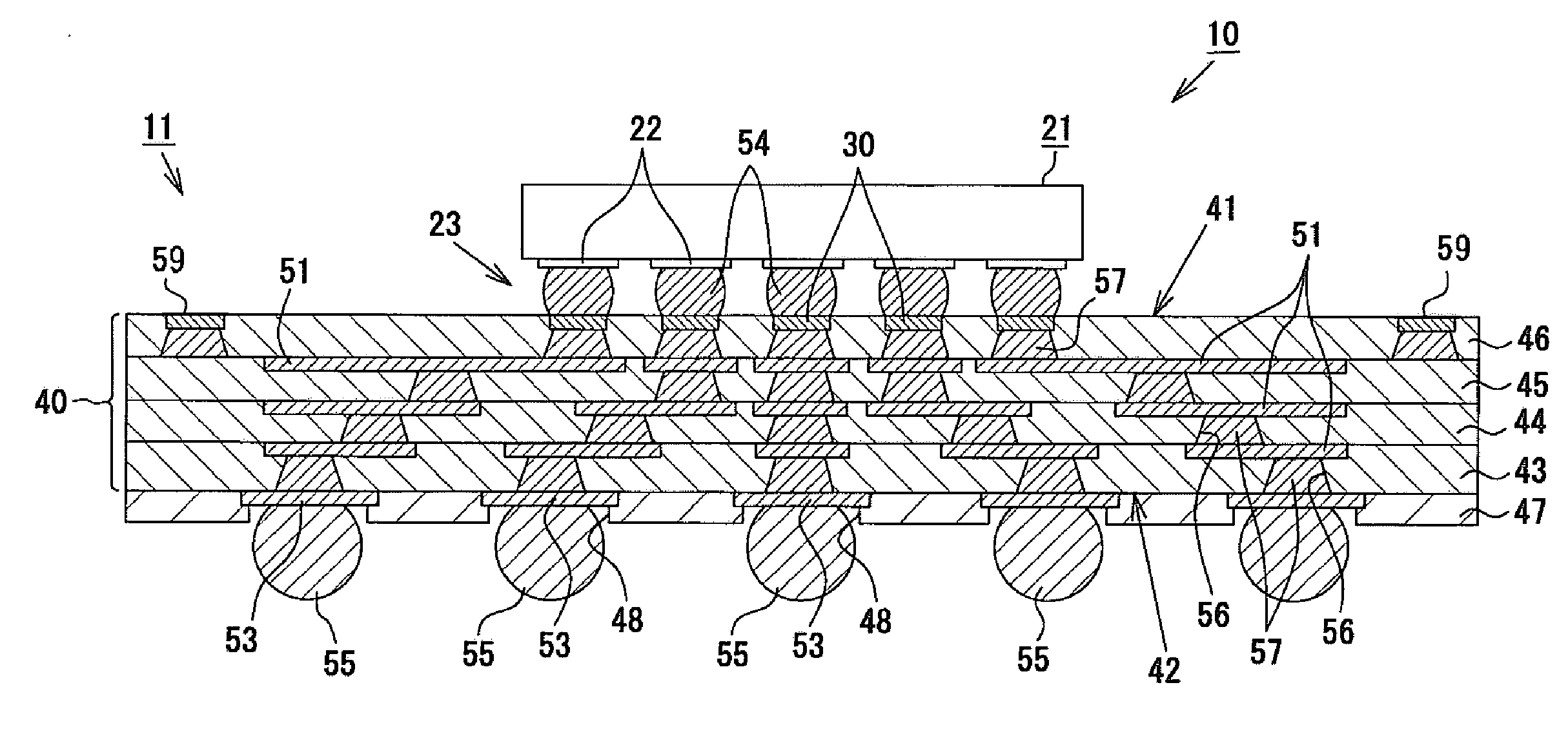
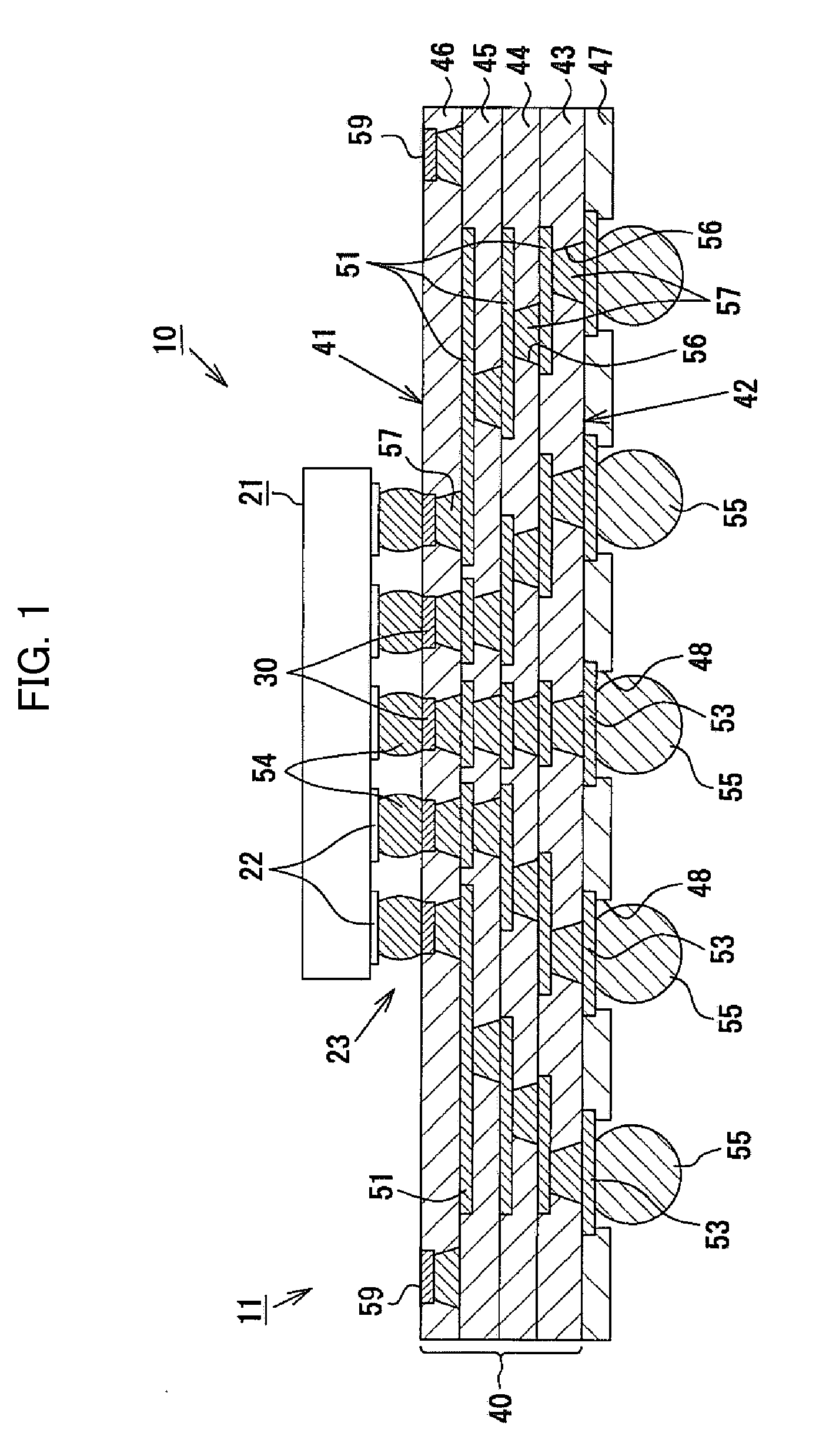
[0060]As shown in FIGS. 1 and 2, the semiconductor package 10 of the present embodiment is of a BGA (ball grid array) type, and is composed of a multilayer wiring substrate 11 and a IC chip 21 (chip component), which is a semiconductor integrated circuit element. Notably, the type of the semiconductor package 10 is not limited to BGA, and may be PGA (pin grid array), LGA (land grid array), or the like. The IC chip 21 is preferably formed of silicon whose coefficient of thermal expansion is 4.2 ppm / ° C. and assumes the form of a rectangular flat plate whose size is 15.0 mm (length)×15.0 mm (width)×0.8 mm (thickness).

[0061]Meanwhile, the exemplary multilayer wiring substrate 11 does not have a core substrate, and has a wiring stacked portion 40 (laminated structure) comp...

second embodiment

2. Second Embodiment

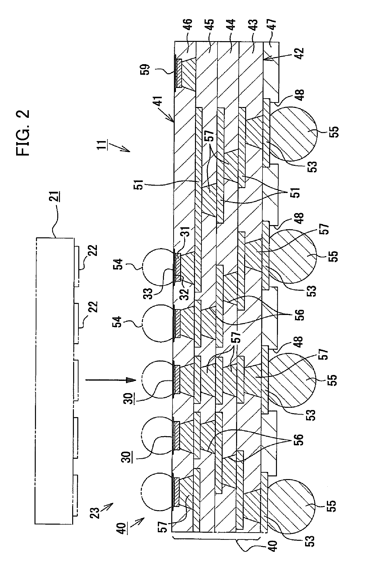
[0086]Next, a second exemplary embodiment of the present invention will be described with reference to FIGS. 21 to 24.

[0087]As shown in FIG. 21, like the terminal pads 30 of the first embodiment, terminal pads 30A of a multilayer wiring substrate 11 of the second embodiment have a structure in which a copper plating layer 31, a nickel plating layer 32, and a gold plating layer 33 are stacked in this sequence, and the gold plating layer 33 has an overhanging portion 33a along the circumference thereof.

[0088]The multilayer wiring substrate 11 having the terminal pads 30A having such a structure can be manufactured by a method which is basically the same as the manufacturing method of the first embodiment. However, a method of forming the overhanging portion 33a in the terminal forming step which is employed in the present embodiment differs from that employed in the first embodiment. That is, a dry film 76 (thickness: about 15 μm), which serves as a resist (mask), ...

third embodiment

3. Third Embodiment

[0091]Next, a third exemplary embodiment of the present invention will be described with reference to FIGS. 25 to 28.

[0092]As shown in FIG. 25, like the terminal pads 30 of the first embodiment, terminal pads 30B of a multilayer wiring substrate 11 of the third embodiment have a structure in which a copper plating layer 31, a nickel plating layer 32, and a gold plating layer 33 are stacked in this sequence, and the gold plating layer 33 has an overhanging portion 33a along the circumference thereof.

[0093]The multilayer wiring substrate 11 having the terminal pads 30B having such a structure can be manufactured by a method which is basically the same as the manufacturing method of the first embodiment. However, a method of forming the overhanging portion 33a in the terminal forming step which is employed in the present embodiment differs from that employed in the first embodiment. That is, a dry film 91 (thickness: about 15 μm), which serves as a resist (first mask...


PUM

PropertyMeasurementUnit
surface roughnessaaaaaaaaaa
sizeaaaaaaaaaa
sizeaaaaaaaaaa

Abstract

A multilayer wiring substrate of the present invention has a laminated structure composed of conductor layers and resin insulating layers stacked alternately. A plurality of surface connection terminals to which terminals of a chip component are to be surface-connected are formed on a main face of the laminated structure. A plurality of via conductors connected to the plurality of surface connection terminals are formed in the resin insulating layers. Each of the plurality of surface connection terminals has a structure in which a copper layer, a nickel layer, and a gold layer are stacked in this sequence. The gold layer is larger in diameter than at least the copper layer. The gold layer has an overhanging portion which extends radially outward from a circumference of the copper layer.

Description

CROSS-REFERENCE TO RELATED APPLICATIONS[0001]This application claims priority to Japanese Patent Application No. JP 2009-33315, filed Feb. 16, 2009, which is hereby incorporated by reference in its entirety.BACKGROUND OF THE INVENTION[0002]1. Field of the Invention[0003]The present invention relates to a multilayer wiring substrate having a laminated structure composed of conductor layers and resin insulating layers alternately stacked, and to a method for manufacturing the same.[0004]2. Description of Related Art[0005]In recent years, semiconductor integrated circuit elements (IC chips) used as microprocessors of computers or the like have been enhanced in speed and function more and more, and, thus, IC chips tend to have an increased number of terminals and a reduced inter-terminal pitch. In general, a large number of terminals are densely disposed in an array on the bottom surface of an IC chip. Such a group of terminals are flip-chip connected to a group of terminals on the moth...

Claims


Application Information

Patent Timeline
Patent Type & Authority Applications(United States)
IPC IPC(8): H05K7/00H05K1/09H05K3/10
CPCH01L21/4857Y10T29/49155H01L24/81H01L2221/68345H01L2224/16H01L2224/81192H01L2224/81801H01L2924/01029H01L2924/01078H01L2924/01079H01L2924/01082H01L2924/01088H01L2924/15174H01L2924/15311H01L2924/30107H05K1/0269H05K1/113H05K3/0097H05K3/205H05K3/243H05K3/3436H05K3/4682H05K2201/09918H05K2201/10674H05K2203/0361H05K2203/0369H05K2203/1184H05K2203/1476H01L2924/01006H01L2924/01024H01L2924/01033H01L2924/1461H01L23/49822H01L2224/16235H01L2924/00H01L2224/0554H01L2224/05568H01L2224/05573H01L2924/00014H01L2924/14H01L2224/05599H01L2224/0555H01L2224/0556
Inventor MAEDA, SHINNOSUKEASANO, TOSHIYAHANDO, TAKUYA
Owner NGK SPARK PLUG CO LTD
Why Eureka
Try Eureka