

Plasma etching method, plasma etching apparatus and storage medium
a plasma etching and plasma technology, applied in the field of plasma etching methods, plasma etching apparatuses and storage media, can solve the problems of warp or deformation of etching shapes, the inability to achieve sufficient modification effect of organic masks by high-speed electrons, and the difficulty of forming etching holes with sufficient etching selectivity
- Summary
- Abstract
- Description
- Claims
- Application Information
AI Technical Summary
Benefits of technology
Problems solved by technology
Method used
Image

Examples
first embodiment
[0064]First, a first embodiment of the present disclosure will be described.
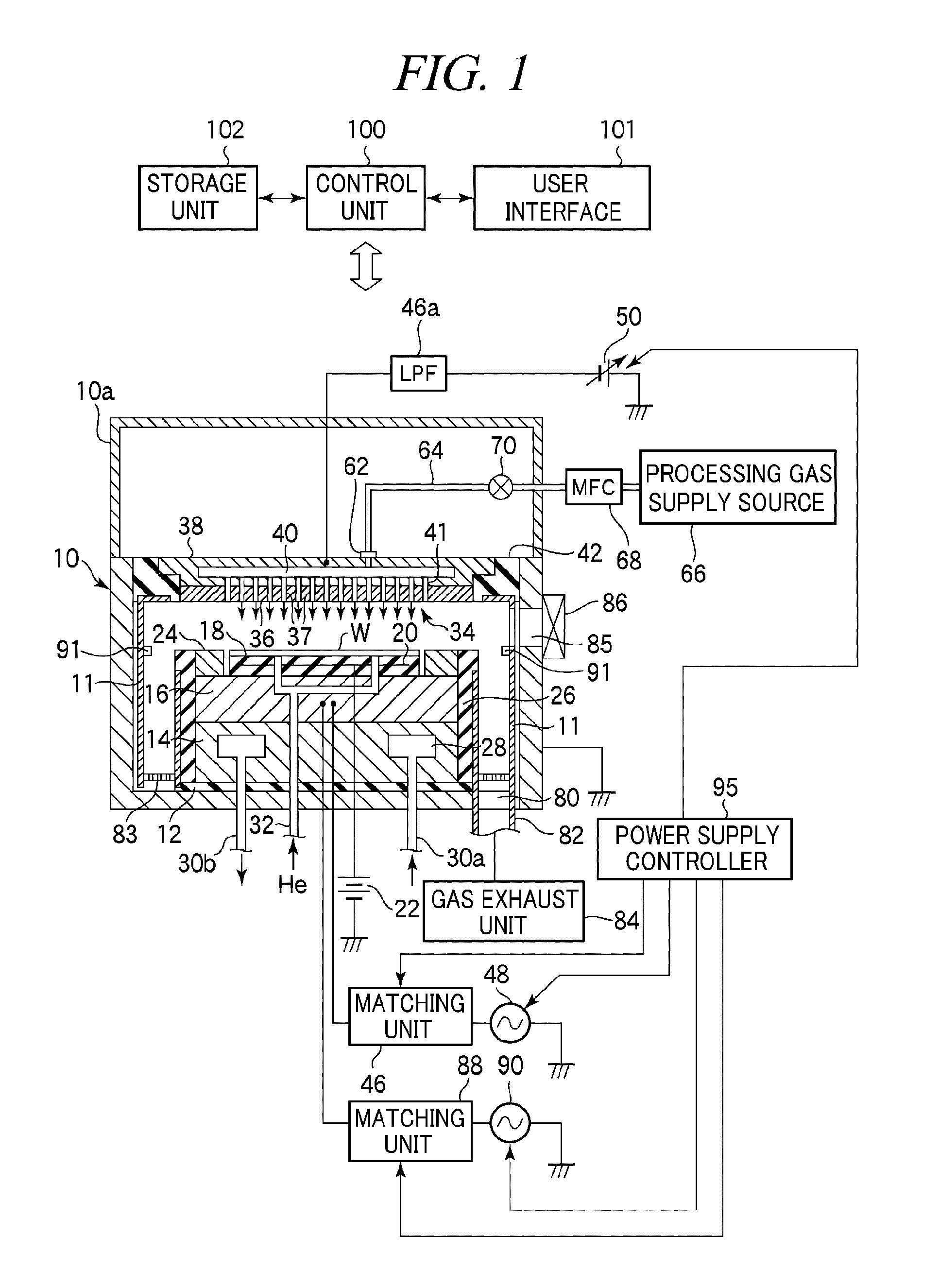
[0065]FIG. 1 is a schematic cross sectional view illustrating an example plasma etching apparatus capable of performing a plasma etching method in accordance with a first embodiment of the present disclosure.
[0066]This plasma etching apparatus is configured as a capacitively coupled parallel plate type plasma etching apparatus and includes a substantially cylindrical chamber (processing vessel) 10 made of, e.g., aluminum with an anodically oxidized surface. The chamber 10 is frame-grounded.
[0067]A cylindrical susceptor support 14 is installed on a bottom of the chamber 10, with an insulating plate 12 made of ceramic therebetween. On the susceptor support 14, a susceptor 16 made of, e.g., aluminum is installed. The susceptor 16 serves as a lower electrode, and a semiconductor wafer W as a target substrate is mounted thereon.
[0068]On a top surface of the susceptor 16, an electrostatic chuck 18 for attracting a...
second embodiment
[0110]Hereinafter, a second embodiment of the present disclosure will be described.
[0111]FIG. 10 is a schematic cross sectional view illustrating an example plasma etching apparatus capable of performing a plasma etching method in accordance with the second embodiment of the present disclosure.
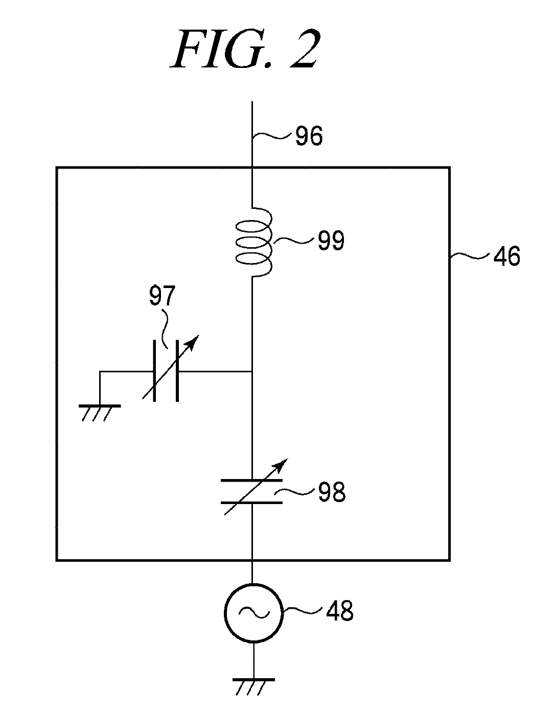
[0112]The plasma etching apparatus shown in FIG. 10 has the same configuration as that of the apparatus shown in FIG. 1 excepting that an anode of a second DC power supply 52 is connected to the side of a susceptor 16 serving as a lower electrode via a low pass filter (LPF) 52a so as to apply a positive (plus) voltage to the susceptor 16 serving as the lower electrode; and the second DC power supply 52 is controlled by a power supply controller 95. Accordingly, in FIG. 10, the same parts as described in FIG. 1 will be assigned same reference numerals, and redundant description will be omitted.
[0113]Now, the plasma etching method in accordance with the second embodiment, which is performed by t...
third embodiment
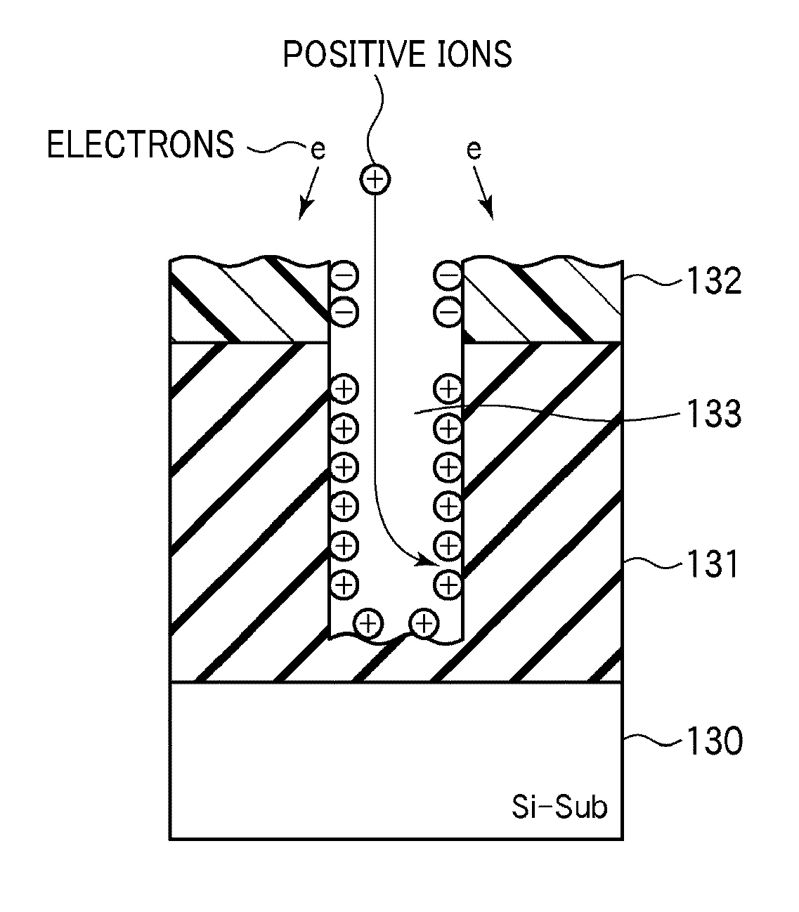
[0132]A third embodiment is described for an example case of performing HARC etching by using the plasma etching apparatus shown in FIG. 1. For example, as in the second embodiment, HARC etching is performed on an insulating film 131 of a semiconductor wafer W having a structure shown in FIG. 11.
[0133]Here, a first process of etching is performed in the same manner as in the second embodiment. Subsequently, a second process of etching is the same as the second process of the etching of the second embodiment excepting that a DC voltage is not applied from the second DC power supply 52 during a plasma-off period.
[0134]That is, as shown in FIG. 21, a plasma-on state in which plasma (glow plasma) is generated by the first high frequency power supply 48 and a plasma-off state in which glow plasma is not generated are alternately repeated. In synchronization with the on and off of the plasma, the first DC power supply 50 applies a negative DC voltage to the upper electrode 34 during both ...
PUM
| Property | Measurement | Unit |
|---|---|---|
| aspect ratio | aaaaa | aaaaa |
| aspect ratio | aaaaa | aaaaa |
| frequency | aaaaa | aaaaa |
Abstract
Description
Claims
Application Information