Method for Forming Porous Insulating Film and Semiconductor Device

a technology of porous insulating film and semiconductor devices, which is applied in the direction of semiconductor devices, semiconductor/solid-state device details, electrical apparatus, etc., can solve the problems of increasing the capacity between wirings, and achieve the effect of improving the performance of wirings and low power consumption

Active Publication Date: 2010-09-02
RENESAS ELECTRONICS CORP
View PDF10 Cites 29 Cited by
  • Summary
  • Abstract
  • Description
  • Claims
  • Application Information

AI Technical Summary

Benefits of technology

[0021]With the use of a method for forming porous insulating film and a semiconductor device according to the present invention, low-dielectric interlayer constant

Problems solved by technology

In recent years, progress in microfabrication of LSI resulted in wirings with finer dimensions, and increased capacity between wir

Method used


Image

  • Method for Forming Porous Insulating Film and Semiconductor Device
  • Method for Forming Porous Insulating Film and Semiconductor Device
  • Method for Forming Porous Insulating Film and Semiconductor Device

Examples


first exemplary embodiment

[0043]In the present invention, in the method for forming porous insulating film preferable for interlayer insulating film by the plasma vapor deposition method while supplying at least cyclic organosiloxane raw material to reaction chamber, forming is made possible with the use of a mixed gas of cyclic organosiloxane raw material and compound raw material.

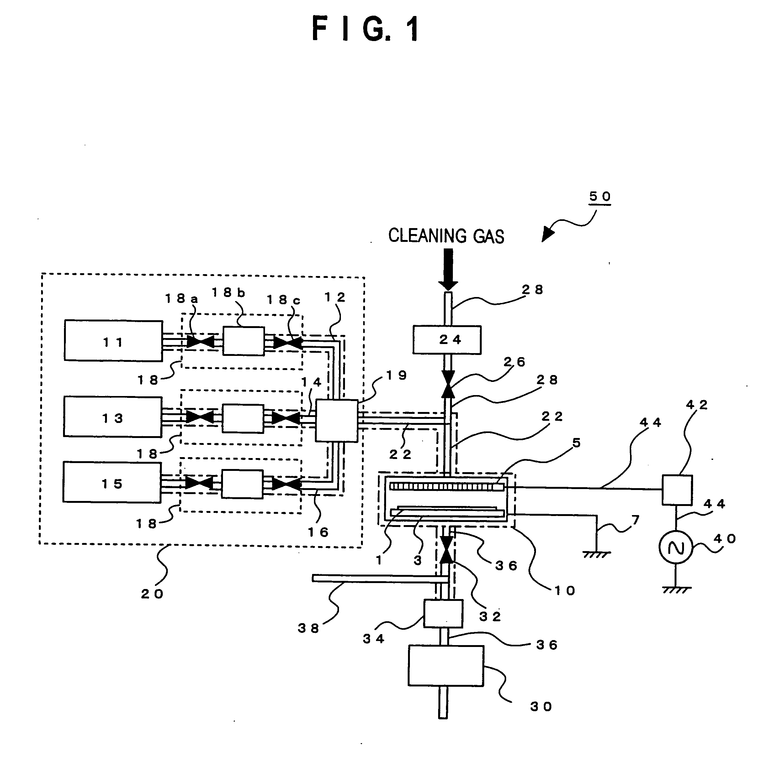
[0044]A first exemplary embodiment for forming porous insulating film while supplying a vaporized raw material supplied to a reaction chamber, will be explained hereunder referring to FIG. 1.

[0045]FIG. 1 is a schematic view showing one example of plasma CVD device which can be used for a forming porous insulating film (film forming) based on the method of the present invention. A plasma CVD device 50 shown in FIG. 1 includes a reaction chamber 10, a gas supplying section 20, a vacuum pump 30, and a high-frequency power supply 40. The gas supplying section 20 is connected to the reaction chamber 10 by a gas supplying pipe 22, and t...

second exemplary embodiment

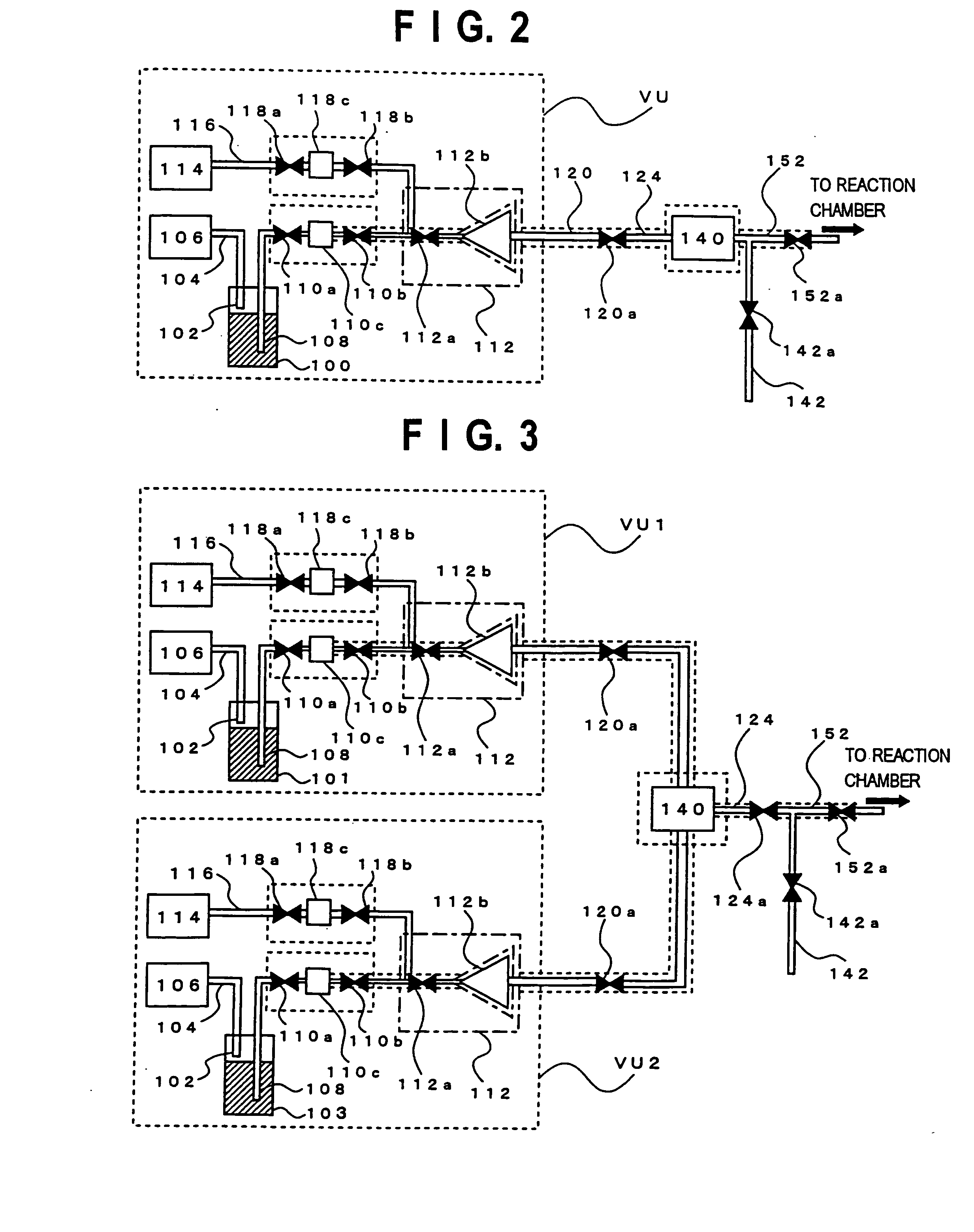
[0054]Hereafter, a second exemplary embodiment of the present invention, in which vaporized raw material is supplied to a reaction chamber to form porous insulating film, will be explained referring to FIG. 2. FIG. 2 is a schematic diagram showing one example of important part of a gas supplying section preferably used for a case where boiling point of cyclic organosiloxane intended to be used as the raw material gas is low, and the cyclic organosiloxane may become liquid state unless artificial heating is provided.

[0055]The cyclic organosiloxane raw material and compound raw material are mixed with arbitrary ratio, and the mixture is supplied from the gas supplying system 20 as mixed raw material 100.

[0056]A vaporization control unit VU includes a raw material tank 102 for accommodating the mixed raw material 100 in liquid state, a pressurized gas supplying device 106 for supplying pressurized gas into a raw material tank 108 via a pressurized gas supplying pipe 104, a mixed raw ma...

third exemplary embodiment

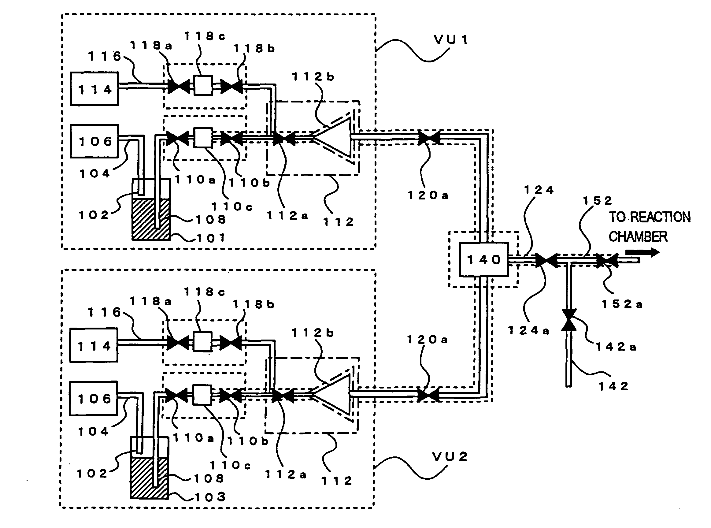
[0063]Hereafter, a third exemplary embodiment of the present invention, in which vaporized raw material is supplied to a reaction chamber to form porous insulating film, will be explained referring to FIG. 3. FIG. 3 is a schematic diagram showing one example of important part of the gas supplying section preferably used for a case where boiling point of cyclic organosiloxane intended to be used as the raw material gas is low, and the cyclic organosiloxane may become liquid state unless artificial heating is provided.

[0064]Cyclic organosiloxane raw material and compound raw material may be prepared in separate raw material tanks and mixed with arbitrary ratio each via a flow meter. Cyclic organosiloxane raw material 101 and compound raw material 103 are supplied from the raw material supplying system 20, respectively.

[0065]A vaporization control unit VU1 includes the raw material tank 102 for accommodating cyclic organosiloxane raw material 101 in liquid state, the pressurized gas su...


PUM


Abstract

A method for forming porous insulating film using cyclic siloxane raw material monomer is provided, which method suppresses detachment of hydrocarbon and is able to form a low-density film.
In a method where at least cyclic organosiloxane raw material 101 is supplied to a reaction chamber and an insulating film is formed by plasma vapor deposition method, above-mentioned problem is solved by a method for a forming porous insulating film using the mixed gas of a cyclic organosiloxane raw material 101 and a compound raw material 103 including a part of chemical structure comprising the cyclic organosiloxane raw material 101. The compound raw material 103 is preferably a compound including a part of side chain of the cyclic organosiloxane raw material 101.

Description

TECHNICAL FIELD [0001]The present invention relates to a method for forming porous insulating film, and in particular, relates to a semiconductor device including a wiring, and a semiconductor device including damascene wiring structure including Cu as principal component.BACKGROUND ART[0002]In silicon semiconductor integrated circuit (LSI), conventionally, aluminum (Al) or Al alloy has been used extensively as the conductive material. With the recent advance in microfabrication technology used in the method for manufacturing of LSI, and for the purpose of reduction in resistance in the wiring and for improvement of reliability, use of copper (Cu) in the conductive material has begun to appear. Since Cu easily diffuses in a silicon oxide film, according to the prior art, conductive barrier metal film for prevention of diffusion of Cu is provided to side face and bottom face of the Cu wiring, and insulating barrier film is employed at top face of the Cu wiring.[0003]In recent years, ...

Claims


Application Information

Patent Timeline
IPC IPC(8): H01L23/29H01L21/47
CPCH01L21/02274H01L21/3122H01L2924/0002H01L21/31695H01L21/76807H01L21/7682H01L21/76835H01L23/53238H01L23/5329H01L23/53295H01L2221/1036H01L21/02126H01L21/02203H01L21/02216H01L2924/00H01L2221/1047
Inventor TADA, MUNEHIROFURUTAKE, NAOYATAKEUCHI, TSUNEOHAYASHI, YOSHIHIRO
Owner RENESAS ELECTRONICS CORP
Why Eureka
Try Eureka