

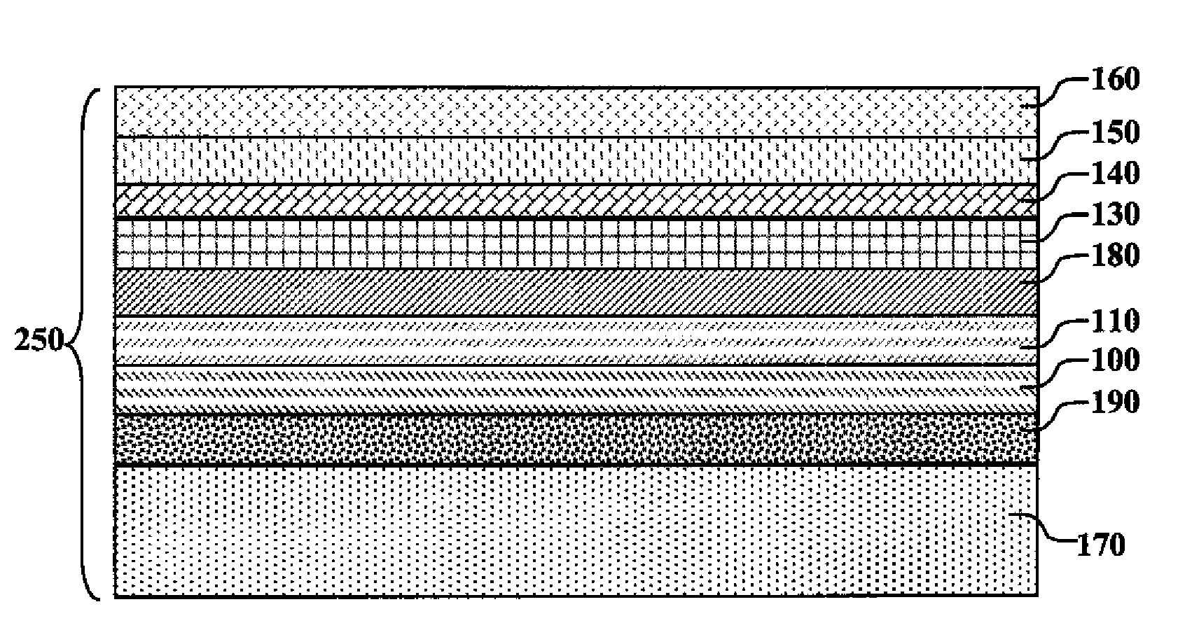
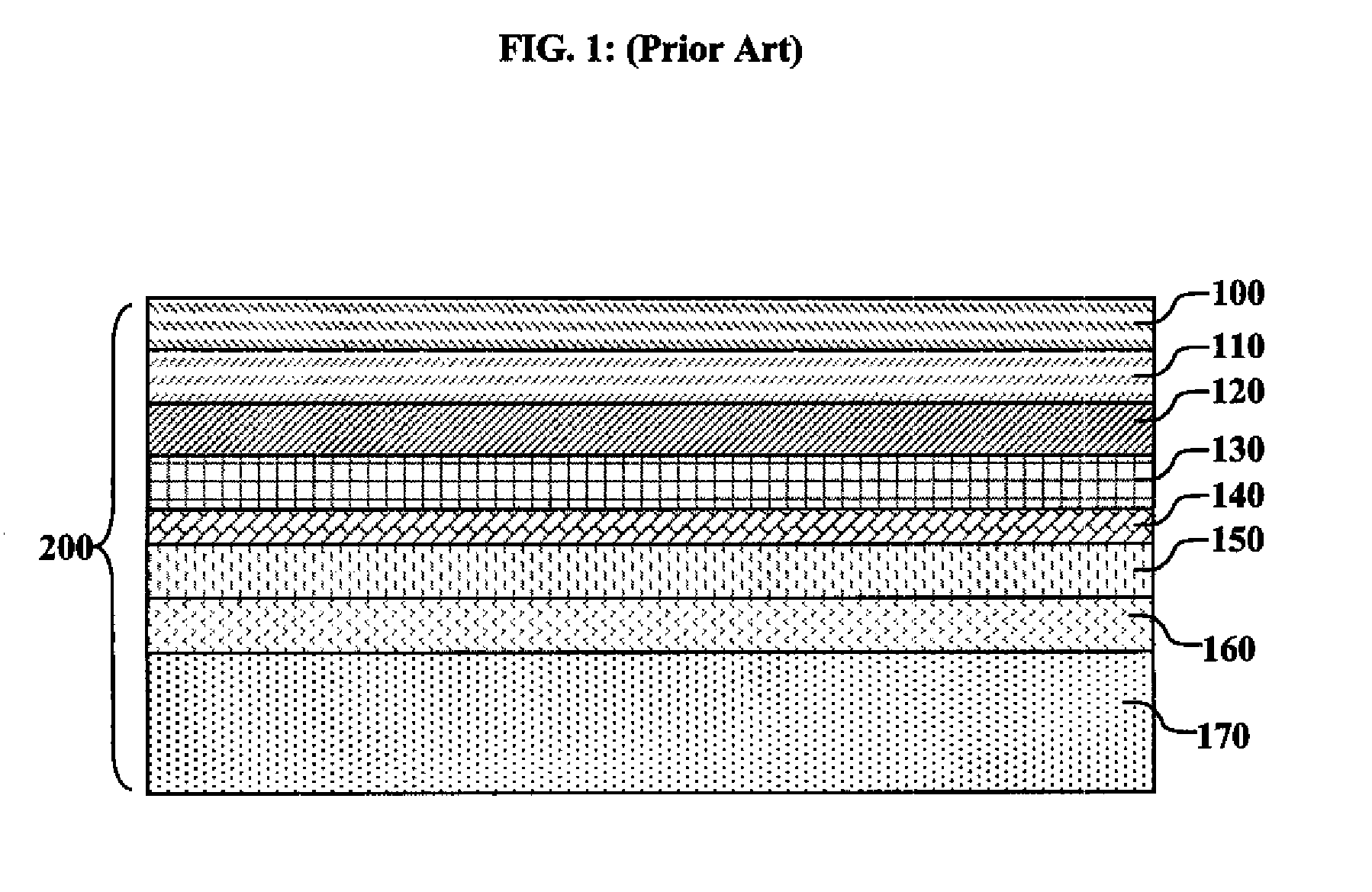
Inverted bottom-emitting OLED device
a bottom-emitting, oled technology, applied in the direction of discharge tube luminescnet screens, discharge tube/lamp details, electric discharge lamps, etc., can solve the problems of extremely high voltage (>100 volts) for el devices to operate, low electron mobility in organic materials, and high resistance in the medium, so as to improve n-type semiconductor compatibility and reduce air sensitivity
- Summary
- Abstract
- Description
- Claims
- Application Information
AI Technical Summary
Benefits of technology
Problems solved by technology
Method used
Image

Examples
example 2 (
Inventive)
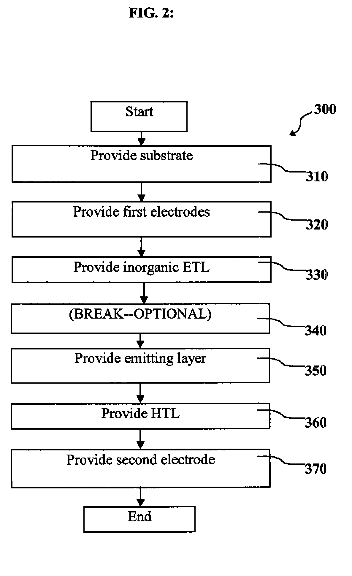
[0050]An OLED device was constructed as described in Example 1, except that the following step was added between Steps 1 and 2:[0051]1a. A 40 nm layer of unpatterned ZnO was deposited uniformly on the substrate.
[0052]After deposition, a positive voltage was applied to the top (anode) electrode and a negative voltage to the bottom (cathode) electrode at a constant current of 20 ma / cm2. Any spectral output was measured. Example 1, the comparative example did not emit. Inventive Example 2 emitted orange light with a spectral maximum at 593 nm wavelength and a luminance of 61 candela / m2. This shows that the zinc oxide layer, which is an electron-transporting layer, enables this device to function.
example 4 (
Inventive)
[0060]An OLED device was constructed as described in Example 3, except that the following step was added between Steps 1 and 2:[0061]1a. A 40 nm layer of unpatterned ZnO was deposited uniformly on the substrate. The sample was briefly dipped in deionized water and then dried before placing in a vacuum chamber.
[0062]After deposition, a positive voltage was applied to the top (anode) electrode and a negative voltage to the bottom (cathode) electrode at a constant current of 20 ma / cm2. Any spectral output was measured. Example 3, the comparative example, did not emit. Inventive Example 4 emitted green light with a spectral maximum at 535 nm wavelength and a luminance of 2800 candela / m2. Example 4 shows the robustness of the completed device to humidity exposure of the intermediate inorganic coated portion of the OLED. This allows one to pre-manufacture a substrate with active matrix electronics and an electron-transporting layer, and store it without extraordinary precautions...
example 6 (
Inventive)
[0070]An OLED device was constructed as described in Example 5, except that the following step was added between Steps 1 and 2:[0071]1a. A 40 nm layer of unpatterned ZnO was deposited uniformly on the substrate.
[0072]After deposition, a positive voltage was applied to the top (anode) electrode and a negative voltage to the bottom (cathode) electrode at a constant current of 20 ma / cm2. Any spectral output was measured. Example 5, the comparative example, did not emit. Inventive Example 6 shows the use of a double emission layer, which provides multiple emission peaks, with the inorganic electron-transporting layer. Example 6 emitted a color of about 0.46 CIEx, 0.46 CIEy, which is an approximation of white, at 20 ma / cm2 and a luminance of 137 candela / m2.
[0073]The invention has been described in detail with particular reference to certain preferred embodiments thereof, but it will be understood that variations and modifications can be effected within the spirit and scope of t...
PUM
 Abstract
Description
Claims
Application Information