MOS capacitor and charge pump with MOS capacitor

a technology of metal oxide semiconductors and capacitors, applied in semiconductor devices, digital storage, instruments, etc., can solve the problems of disadvantages of capacitor c implemented with the pmosfet b>110/b>, and the malfunction of the charge pump b>100/b>, and achieve the effect of stable capacitance in the charge pump and enhanced performan

Inactive Publication Date: 2010-09-09
SAMSUNG ELECTRONICS CO LTD
View PDF4 Cites 35 Cited by
  • Summary
  • Abstract
  • Description
  • Claims
  • Application Information

AI Technical Summary

Benefits of technology

[0011]Accordingly, a MOS (metal oxide semiconductor) capacitor is formed with a multiple-

Problems solved by technology

The capacitor C implemented with the PMOSFET 110 is disadvantageous because the capacitance of the capacitor C is decreased near the threshold voltage of the PMOSFET

Method used


Image

  • MOS capacitor and charge pump with MOS capacitor
  • MOS capacitor and charge pump with MOS capacitor
  • MOS capacitor and charge pump with MOS capacitor

Examples


Embodiment Construction

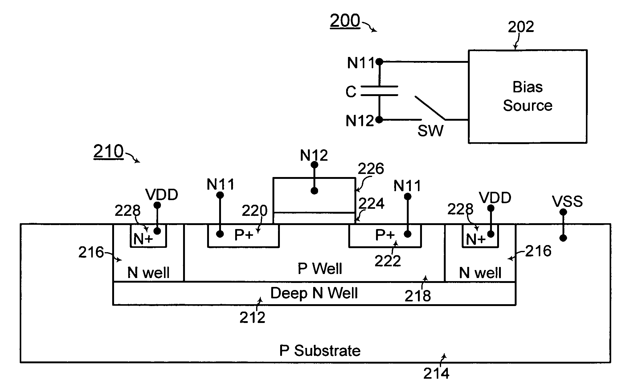
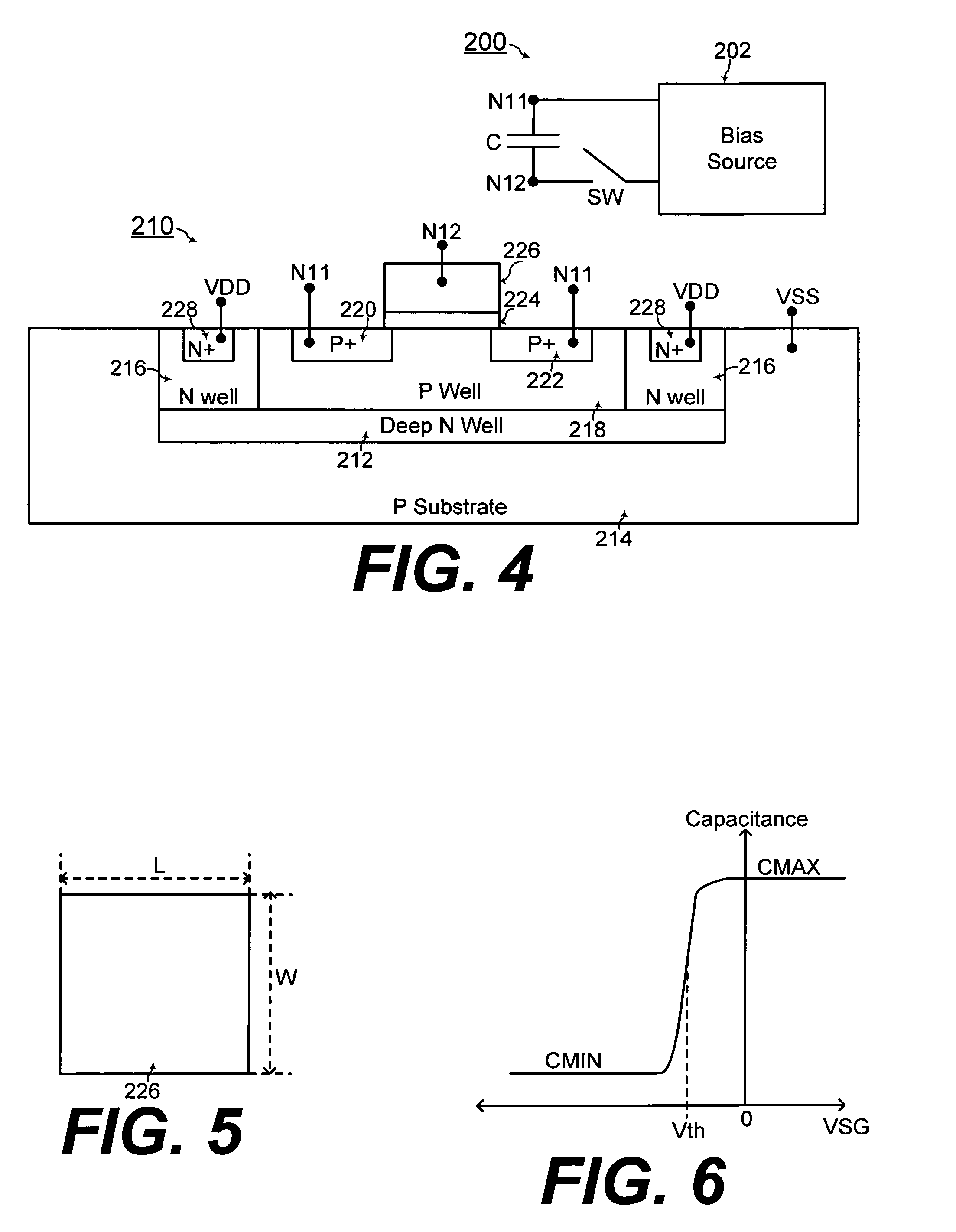
[0042]FIG. 4 shows a block diagram of a charge pump 200 with a cross-sectional view of a MOS (metal oxide semiconductor) device 210 having a multiple-well structure for forming a capacitor C of the charge pump 200, according to an embodiment of the present invention. The charge pump 200 further includes a bias source 202 coupled to a first node N11 of the capacitor C and coupled to a second node N12 of the capacitor C via a switch SW.

[0043]Further referring to FIG. 4, the MOS device 210 includes a deep well 212 formed in a semiconductor substrate 214. The MOS device 210 further includes at least one side well 216 formed to abut the deep well 212. The MOS device 210 also includes a P well 218 forming a device body of the MOS device 210.

[0044]Also in FIG. 4, the MOS device 210 includes a first body bias region 220 and a second body bias region 222 formed in the P well 218 for providing low resistance contact and biasing of the P well 218. A gate dielectric 224 is formed over a channel...


PUM


Abstract

A MOS capacitor in a charge pump includes a MOS device with at least one body bias region and a device body of a same conductivity type for providing maximum capacitance over a wide voltage range. The MOS capacitor also includes a gate forming a first terminal of the MOS capacitor, and the at least one body bias region forms a second terminal of the MOS capacitor. The MOS capacitor further includes a multiple-well structure formed with the device body and a deep well in a substrate for enhanced noise immunity.

Description

CROSS-REFERENCE TO RELATED APPLICATION(S)[0001]The present application claims priority under 35 U.S.C. § 119 to Korean Patent Application No. 10-2009-0018110, filed on Mar. 3, 2009, which is incorporated herein by reference in its entirety.TECHNICAL FIELD[0002]The present invention relates generally to MOS (metal oxide semiconductor) capacitors and charge pumps, and more particularly, to a charge pump having a MOS capacitor with a multiple-well structure for providing voltage in a semiconductor device such as a memory device for example.BACKGROUND OF THE INVENTION[0003]A charge pump is commonly used in a semiconductor device such as a memory device for providing a voltage with high magnitude above that provided by a power source. For example, a memory device such as a DRAM (dynamic random access memory) device, a EEPROM (electrically erasable and programmable read only memory) device, or a flash memory device commonly has charge pumps for providing voltages used to write, read, and / ...

Claims


Application Information

Patent Timeline
IPC IPC(8): G11C11/24G11C5/14G05F1/10H01L29/94
CPCG11C5/145H01L29/94H01L29/66181H01L21/265H01L21/18
Inventor JUNG, SANG-HEEKIM, YOUNG-KWAN
Owner SAMSUNG ELECTRONICS CO LTD
Why Eureka
Try Eureka